tmc5130
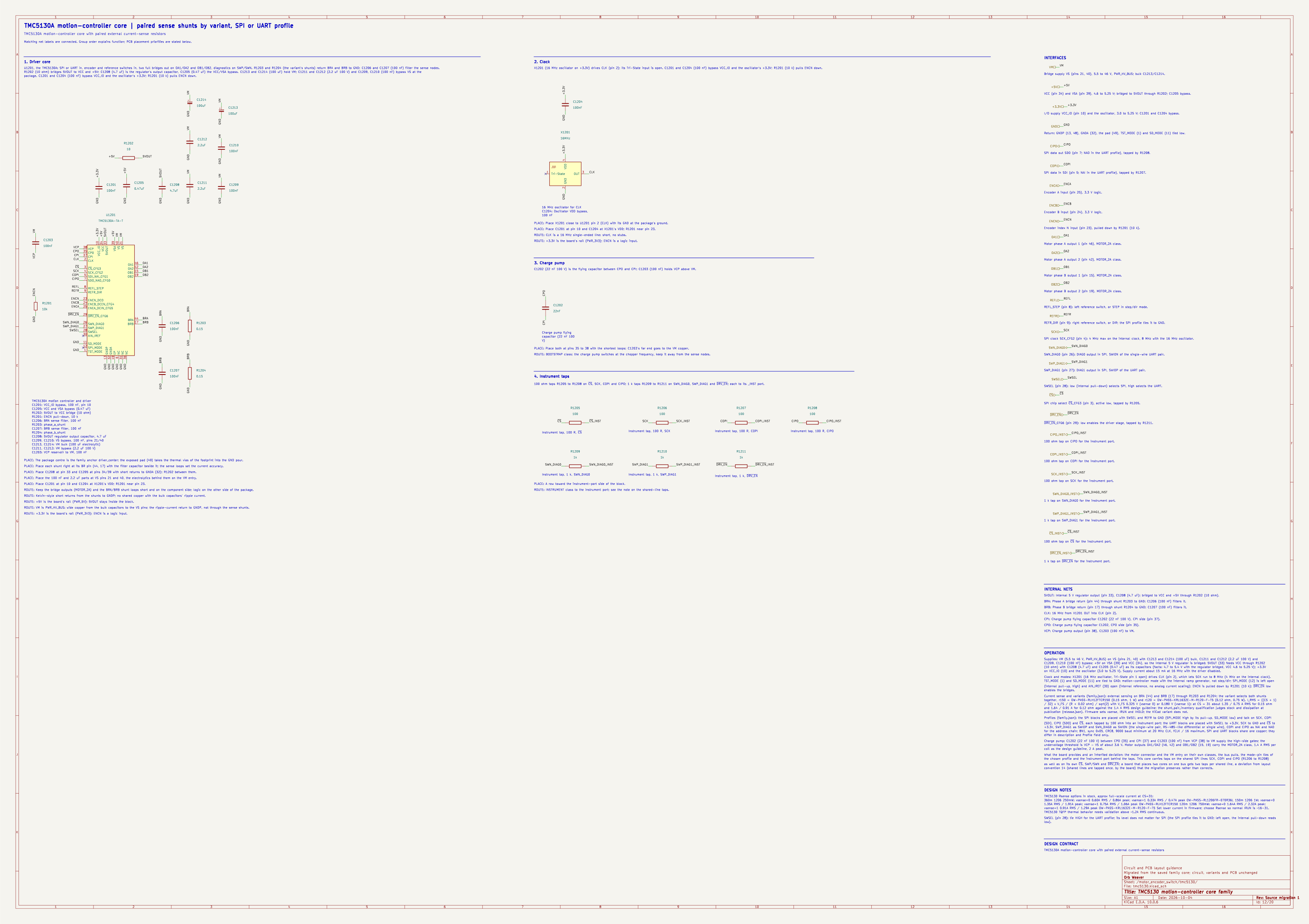
Block orb_weaver_tmc5130:tmc5130_spi_r150 placed in /motor_encoder_switch of mouse-joystick-pcb. TMC5130A motion-controller core with paired external current-sense resistors
| Lifecycle | routed |
| Family | tmc5130 r150 (spi): OW-PASS-RLH12FTCR150 |
| Placement | anchor (1, -14) mm, rotation 90°, front side; anchor rule: inferred (block not in the anchor table): the footprint with most pads |
| Sheet | tmc5130.kicad_sch; sheet pins: the library's arrangement |
| Drawing | mouse-joystick-pcb-motor_encoder_switch-tmc5130.svg |
On the Board
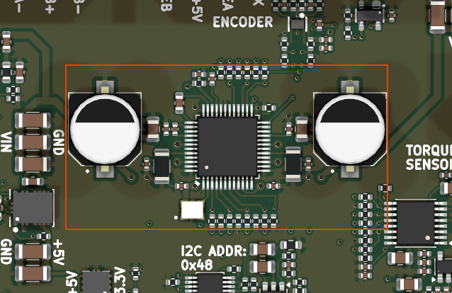
Block 7 of the board view: 36.8 × 18.9 mm on the top side, its centre 1.0 mm right of and 14.0 mm above the board centre (X right, Y up, as the enclosure tables); 27 footprints. The picture is the top render clipped around the block, the rectangle the extent of its footprints' courtyards.
Description
TMC5130A SPI r150: paired 0.15 ohm shunts; set firmware vsense and IRUN/IHOLD for motor; hardware qualification pending. SPI profile. board connections: SWSEL to GND, REFR to GND. SPI_MODE high (existing internal pull-up). SD_MODE low. Configure vsense and IRUN/IHOLD for the selected shunts and motor
Ports
The brief's shape, edge, class and meaning for each port, then what the board wires it to.
| Port | Shape | Edge | Class | Wired to | Board net | Board class | GPIO | Meaning | On this board |
|---|---|---|---|---|---|---|---|---|---|
+3.3V |
passive | west | PWR_3V3 | +3.3V |
/+3.3V_SW |
PWR_3V3 | I/O supply VCC_IO (pin 10) and the oscillator, 3.0 to 5.25 V; C4001 and C4004 bypass. | ||
+5V |
passive | west | PWR_5V | +5V |
/+5V_SW |
PWR_5V | VCC (pin 34) and VSA (pin 39), 4.6 to 5.25 V; bridged to 5VOUT through R4002; C4005 bypass. | ||
CIPO |
output | west | Default | TMC_SPI_CIPO |
/TMC_SPI_CIPO |
Default | GP4 |
SPI data out SDO (pin 7; NAO in the UART profile), tapped by R4008. | Driver SPI CIPO (SPI0 RX); in as the MCU sees it, via the bus switch |
CIPO_INST |
output | west | INSTRUMENT | TMC_SPI_CIPO_INST |
/TMC_SPI_CIPO_INST |
INSTRUMENT | 100 ohm tap on CIPO for the instrument port. | ||
COPI |
input | west | Default | TMC_SPI_COPI |
/TMC_SPI_COPI |
Default | GP7 |
SPI data in SDI (pin 5; NAI in the UART profile), tapped by R4007. | Driver SPI COPI (SPI0 TX); out as the MCU sees it, via the bus switch |
COPI_INST |
output | west | INSTRUMENT | TMC_SPI_COPI_INST |
/TMC_SPI_COPI_INST |
INSTRUMENT | 100 ohm tap on COPI for the instrument port. | ||
ENCA |
input | west | Default | ENCA |
/motor_encoder_switch/ENCA |
Default | Encoder A input (pin 25), 3.3 V logic. | ||
ENCB |
input | west | Default | ENCB |
/motor_encoder_switch/ENCB |
Default | Encoder B input (pin 24), 3.3 V logic. | ||
ENCN |
input | west | Default | open: no-connect flag | Encoder index N input (pin 23), pulled down by R4001 (10 k). | ||||
GND |
passive | west | PWR_RETURN_LOCAL | GND |
/GND |
PWR_RETURN_LOCAL | Return: GNDP (13, 48), GNDA (32), the pad (49), TST_MODE (1) and SD_MODE (11) tied low. | ||
OA1 |
passive | west | MOTOR_2A | OA1 |
/motor_encoder_switch/OA1 |
MOTOR_2A | Motor phase A output 1 (pin 46), MOTOR_2A class. | ||
OA2 |
passive | west | MOTOR_2A | OA2 |
/motor_encoder_switch/OA2 |
MOTOR_2A | Motor phase A output 2 (pin 42), MOTOR_2A class. | ||
OB1 |
passive | west | MOTOR_2A | OB1 |
/motor_encoder_switch/OB1 |
MOTOR_2A | Motor phase B output 1 (pin 15), MOTOR_2A class. | ||
OB2 |
passive | west | MOTOR_2A | OB2 |
/motor_encoder_switch/OB2 |
MOTOR_2A | Motor phase B output 2 (pin 19), MOTOR_2A class. | ||
REFL |
input | west | Default | LIMIT_SW |
/motor_encoder_switch/LIMIT_SW |
Default | REFL_STEP (pin 8): left reference switch, or STEP in step/dir mode. | ||
REFR |
input | west | Default | GND |
/GND |
PWR_RETURN_LOCAL | REFR_DIR (pin 9): right reference switch, or DIR; the SPI profile ties it to GND. | ||
SCK |
input | west | Default | TMC_SPI_SCK |
/TMC_SPI_SCK |
Default | GP6 |
SPI clock SCK_CFG2 (pin 4): 4 MHz max on the internal clock, 8 MHz with the 16 MHz oscillator. | Driver SPI clock (SPI0 SCK); out as the MCU sees it, via the bus switch |
SCK_INST |
output | west | INSTRUMENT | TMC_SPI_SCK_INST |
/TMC_SPI_SCK_INST |
INSTRUMENT | 100 ohm tap on SCK for the instrument port. | ||
SWN_DIAG0 |
bidirectional | west | Default | DIAG0 |
/TMC_DIAG0 |
Default | GP5 |
SWN_DIAG0 (pin 26): DIAG0 output in SPI, SWION of the single-wire UART pair. | Driver diagnostic 0; in as the MCU sees it, via the bus switch |
SWN_DIAG0_INST |
output | west | INSTRUMENT | DIAG0_INST |
/TMC_DIAG0_INST |
INSTRUMENT | 1 k tap on SWN_DIAG0 for the instrument port. | ||
SWP_DIAG1 |
bidirectional | west | Default | DIAG1 |
/TMC_DIAG1 |
Default | GP8 |
SWP_DIAG1 (pin 27): DIAG1 output in SPI, SWIOP of the UART pair. | Driver diagnostic 1; in as the MCU sees it, via the bus switch |
SWP_DIAG1_INST |
output | west | INSTRUMENT | DIAG1_INST |
/TMC_DIAG1_INST |
INSTRUMENT | 1 k tap on SWP_DIAG1 for the instrument port. | ||
SWSEL |
input | west | Default | open: no-connect flag | SWSEL (pin 28): low (internal pull-down) selects SPI, high selects the UART. | ||||
VM |
passive | west | PWR_HV_BUS | VM |
/+36V_SW |
PWR_HV_BUS | Bridge supply VS (pins 21, 40), 5.5 to 46 V, PWR_HV_BUS; bulk C4013/C4014. | ||
~{CS} |
input | west | Default | ~{TMC_CS} |
/~{TMC_CS} |
Default | GP2 |
SPI chip select ~{CS}_CFG3 (pin 3), active low, tapped by R4005. | Driver chip select; out as the MCU sees it, via the bus switch |
~{CS}_INST |
output | west | INSTRUMENT | ~{TMC_CS}_INST |
/~{TMC_CS}_INST |
INSTRUMENT | 100 ohm tap on ~{CS} for the instrument port. | ||
~{DRV_EN} |
input | west | Default | ~{DRV_EN} |
/~{TMC_DRV_EN} |
Default | GP3 |
~{DRV_EN}_CFG6 (pin 29): low enables the driver stage, tapped by R4011. | Driver enable, active low; out as the MCU sees it, via the bus switch |
~{DRV_EN}_INST |
output | west | INSTRUMENT | ~{DRV_EN}_INST |
/~{TMC_DRV_EN}_INST |
INSTRUMENT | 1 k tap on ~{DRV_EN} for the instrument port. |
Parts
As placed on the board's sheet; 27 of 27 paired with the brief's references by symbol identity, the rest given the brief's role where the internal part has one, else the catalog's role slug; the placement is the Placement field of the board's symbol, else of the library's (D38); the manufacturer part and the LCSC number are the board's BOM's.
| Reference | Brief | Part | Value | Role | Placement | Manufacturer part | LCSC | DNP |
|---|---|---|---|---|---|---|---|---|
C1201 |
C4001 |
OW-CAP-100N-0402-X5R-16V |
100nF | VCC_IO bypass, 100 nF, pin 10 | beside U1201.10 (VCC_IO), on +3.3V | GRM155R62A104KE14D | C162178 | |
C1202 |
C4002 |
OW-PASS-GCM188R72A223KA37D |
22nF | Charge pump flying capacitor (22 nF 100 V) | GCM188R72A223KA37D | C161234 | ||
C1203 |
C4003 |
OW-CAP-100N-0402-X5R-16V |
100nF | VCP reservoir to VM, 100 nF | beside U1201.38 (VCP), on VCP | GRM155R62A104KE14D | C162178 | |
C1204 |
C4004 |
OW-CAP-100N-0402-X5R-16V |
100nF | Oscillator VDD bypass, 100 nF | beside X1201.4 (VDD), on +3.3V | GRM155R62A104KE14D | C162178 | |
C1205 |
C4005 |
OW-PASS-GRT155R6YA474KE01D |
0.47uF | VCC and VSA bypass (0.47 uF) | beside U1201.34 (VCC), on +5V | GRT155R6YA474KE01D | C711580 | |
C1206 |
C4006 |
OW-CAP-100N-0402-X5R-16V |
100nF | BRA sense filter, 100 nF | beside U1201.44 (BRA), on BRA | GRM155R62A104KE14D | C162178 | |
C1207 |
C4007 |
OW-CAP-100N-0402-X5R-16V |
100nF | BRB sense filter, 100 nF | beside U1201.17 (BRB), on BRB | GRM155R62A104KE14D | C162178 | |
C1208 |
C4008 |
OW-CAP-4U7-0402-X5R-16V |
4.7uF | 5VOUT regulator output capacitor, 4.7 uF | beside U1201.33 (5VOUT), on 5VOUT | GRM155R61E475ME15D | C2858031 | |
C1209 |
C4009 |
OW-CAP-100N-0402-X5R-16V |
100nF | VS bypass, 100 nF, pins 21/40 | beside U1201.21 (VS), on VM | GRM155R62A104KE14D | C162178 | |
C1210 |
C4010 |
OW-CAP-100N-0402-X5R-16V |
100nF | VS bypass, 100 nF, pins 21/40 | beside U1201.21 (VS), on VM | GRM155R62A104KE14D | C162178 | |
C1211 |
C4011 |
OW-PASS-GRM21BD72A225KE01L |
2.2uF | VM bypass (2.2 uF 100 V) | beside U1201.40 (VS), on VM | GRM21BD72A225KE01L | C2981733 | |
C1212 |
C4012 |
OW-PASS-GRM21BD72A225KE01L |
2.2uF | VM bypass (2.2 uF 100 V) | beside U1201.40 (VS), on VM | GRM21BD72A225KE01L | C2981733 | |
C1213 |
C4013 |
OW-PASS-EEEHAH101UAP |
100uF | VM bulk (100 uF electrolytic) | beside U1201.21 (VS), on VM | EEEHAH101UAP | C336425 | |
C1214 |
C4014 |
OW-PASS-EEEHAH101UAP |
100uF | VM bulk (100 uF electrolytic) | beside U1201.40 (VS), on VM | EEEHAH101UAP | C336425 | |
R1201 |
R4001 |
OW-RES-10K-0402 |
10k | ENCN pull-down, 10 k | beside U1201.23 (ENCN_DCO), on ENCN | ERJ2GEJ103X | C278577 | |
R1202 |
R4002 |
OW-PASS-RC0402FR-0710RL |
10 | 5VOUT to VCC bridge (10 ohm) | beside U1201.34 (VCC), on +5V | RC0402FR-0710RL | C138066 | |
R1203 |
R4003 |
OW-PASS-RLH12FTCR150 |
0.15 | phase_a_shunt | beside U1201.44 (BRA), on BRA | RLH12FTCR150 | C2683383 | |
R1204 |
R4004 |
OW-PASS-RLH12FTCR150 |
0.15 | phase_b_shunt | beside U1201.17 (BRB), on BRB | RLH12FTCR150 | C2683383 | |
R1205 |
R4005 |
OW-PASS-0402WGF1000TCE |
100 | Instrument tap, 100 R, ~{CS} | 0402WGF1000TCE | C25076 | ||
R1206 |
R4006 |
OW-PASS-0402WGF1000TCE |
100 | Instrument tap, 100 R, SCK | 0402WGF1000TCE | C25076 | ||
R1207 |
R4007 |
OW-PASS-0402WGF1000TCE |
100 | Instrument tap, 100 R, COPI | 0402WGF1000TCE | C25076 | ||
R1208 |
R4008 |
OW-PASS-0402WGF1000TCE |
100 | Instrument tap, 100 R, CIPO | 0402WGF1000TCE | C25076 | ||
R1209 |
R4009 |
OW-PASS-RC0402FR-071KL |
1k | Instrument tap, 1 k, SWN_DIAG0 | RC0402FR-071KL | C106235 | ||
R1210 |
R4010 |
OW-PASS-RC0402FR-071KL |
1k | Instrument tap, 1 k, SWP_DIAG1 | RC0402FR-071KL | C106235 | ||
R1211 |
R4011 |
OW-PASS-RC0402FR-071KL |
1k | Instrument tap, 1 k, ~{DRV_EN} | RC0402FR-071KL | C106235 | ||
U1201 |
U4001 |
OW-PWR-TMC5130A-TA-T |
TMC5130A-TA-T | TMC5130A motion controller and driver | TMC5130A-TA-T | C188832 | ||
X1201 |
X4001 |
OW-PASS-ECS-2520S33-160-FN-TR |
16MHz | 16 MHz oscillator for CLK | ECS-2520S33-160-FN-TR | C2451298 |
Operating Notes
- Supplies: VM (5.5 to 46 V, PWR_HV_BUS) on VS (pins 21, 40) with C4013 and C4014 (100 uF) bulk, C4011 and C4012 (2.2 uF 100 V) and C4009, C4010 (100 nF) bypass; +5V on VSA (39) and VCC (34), so the internal 5 V regulator is bridged: 5VOUT (33) feeds VCC through R4002 (10 ohm) with C4008 (4.7 uF) and C4005 (0.47 uF) as its capacitors (facts: 4.7 to 5.4 V with the regulator bridged, VCC 4.6 to 5.25 V); +3.3V on VCC_IO (10) and the oscillator (3.0 to 5.25 V). Supply current about 15 mA at 16 MHz with the driver disabled.
- Clock and modes: X4001 (16 MHz oscillator, Tri-State pin 1 open) drives CLK (pin 2), which lets SCK run to 8 MHz (4 MHz on the internal clock). TST_MODE (1) and SD_MODE (11) are tied to GND: motion-controller mode with the internal ramp generator, not step/dir; SPI_MODE (12) is left open (internal pull-up, high) and AIN_IREF (30) open (internal reference, no analog current scaling); ENCN is pulled down by R4001 (10 k); ~{DRV_EN} low enables the bridges.
- Current sense and variants (family.json): external sensing on BRA (44) and BRB (17) through R4003 and R4004; the variant selects both shunts together, r150 = OW-PASS-RLH12FTCR150 (0.15 ohm, 1 W) and r120 = OW-PASS-KRL1632E-M-R120-F-T5 (0.12 ohm, 0.75 W). I_RMS = ((CS + 1) / 32) x V_FS / (R + 0.02 ohm) / sqrt(2) with V_FS 0.325 V (vsense 0) or 0.180 V (vsense 1): at CS = 31 about 1.35 / 0.75 A RMS for 0.15 ohm and 1.64 / 0.91 A for 0.12 ohm against the 1.4 A RMS design guideline; the shunt_pair_inventory qualification judges stock and dissipation at publication (release.json). Firmware sets vsense, IRUN and IHOLD; the KiCad variant does not.
- Profiles (family.json): the SPI blocks are placed with SWSEL and REFR to GND (SPI_MODE high by its pull-up, SD_MODE low) and talk on SCK, COPI (SDI), CIPO (SDO) and ~{CS}, each tapped by 100 ohm into an instrument port; the UART blocks are placed with SWSEL to +3.3V, SCK to GND and ~{CS} to +3.3V, SWP_DIAG1 as SWIOP and SWN_DIAG0 as SWION (the single-wire pair, RS-485-like differential or single wire), COPI and CIPO as NAI and NAO for the address chain; 8N1, sync 0x05, CRC8, 9000 baud minimum at 20 MHz CLK, fCLK / 16 maximum. SPI and UART blocks share one copper; they differ in description and Profile field only.
- Charge pump: C4002 (22 nF 100 V) between CPO (35) and CPI (37) and C4003 (100 nF) from VCP (38) to VM supply the high-side gates; the undervoltage threshold is VCP - VS of about 3.6 V. Motor outputs OA1/OA2 (46, 42) and OB1/OB2 (15, 19) carry the MOTOR_2A class, 1.4 A RMS per coil as the design guideline, 2 A peak.
- What the board provides and an inherited deviation: the motor connector and the VM entry on their own classes, the bus pulls, the mode-pin ties of the chosen profile and the instrument port behind the taps. This core carries taps on the shared SPI lines SCK, COPI and CIPO (R4006 to R4008) as well as on its own ~{CS}, SWP/SWN and ~{DRV_EN}; a board that places two cores on one bus gets two taps per shared line, a deviation from layout convention 14 (shared lines are tapped once, by the board) that the migration preserves rather than corrects.
Placement and Routing
Driver core
U4001, C4001, C4005, R4002, R4001, C4006, C4007, C4008, C4009, C4010, C4011, C4012, C4013, C4014, R4003, R4004, C4003
U4001, the TMC5130A: SPI or UART in, encoder and reference switches in, two full bridges out on OA1/OA2 and OB1/OB2, diagnostics on SWP/SWN. R4003 and R4004 (the variant's shunts) return BRA and BRB to GND; C4006 and C4007 (100 nF) filter the sense nodes. R4002 (10 ohm) bridges 5VOUT to VCC and +5V; C4008 (4.7 uF) is the regulator's output capacitor, C4005 (0.47 uF) the VCC/VSA bypass. C4013 and C4014 (100 uF) hold VM; C4011 and C4012 (2.2 uF 100 V) and C4009, C4010 (100 nF) bypass VS at the package. C4001 and C4004 (100 nF) bypass VCC_IO and the oscillator's +3.3V; R4001 (10 k) pulls ENCN down.
- Place: The package centre is the family anchor driver_center; the exposed pad (49) takes the thermal vias of the footprint into the GND pour.
- Place: Place each shunt right at its BR pin (44, 17) with the filter capacitor beside it; the sense loops set the current accuracy.
- Place: Place C4008 at pin 33 and C4005 at pins 34/39 with short returns to GNDA (32); R4002 between them.
- Place: Place the 100 nF and 2.2 uF parts at VS pins 21 and 40, the electrolytics behind them on the VM entry.
- Place: Place C4001 at pin 10 and C4004 at X4001's VDD; R4001 near pin 23.
- Route: Keep the bridge outputs (MOTOR_2A) and the BRA/BRB shunt loops short and on the component side; logic on the other side of the package.
- Route: Kelvin-style short returns from the shunts to GNDP; no shared copper with the bulk capacitors' ripple current.
- Route: +5V is the board's rail (PWR_5V); 5VOUT stays inside the block.
- Route: VM is PWR_HV_BUS: wide copper from the bulk capacitors to the VS pins; the ripple-current return to GNDP, not through the sense shunts.
- Route: +3.3V is the board's rail (PWR_3V3); ENCN is a logic input.
Clock
X4001, C4004
X4001 (16 MHz oscillator on +3.3V) drives CLK (pin 2); its Tri-State input is open. C4001 and C4004 (100 nF) bypass VCC_IO and the oscillator's +3.3V; R4001 (10 k) pulls ENCN down.
- Place: Place X4001 close to U4001 pin 2 (CLK) with its GND at the package's ground.
- Place: Place C4001 at pin 10 and C4004 at X4001's VDD; R4001 near pin 23.
- Route: CLK is a 16 MHz single-ended line: short, no stubs.
- Route: +3.3V is the board's rail (PWR_3V3); ENCN is a logic input.
Charge pump
C4002
C4002 (22 nF 100 V) is the flying capacitor between CPO and CPI; C4003 (100 nF) holds VCP above VM.
- Place: Place both at pins 35 to 38 with the shortest loops; C4003's far end goes to the VM copper.
- Route: BOOTSTRAP class; the charge pump switches at the chopper frequency, keep it away from the sense nodes.
Instrument taps
R4005, R4006, R4007, R4008, R4009, R4010, R4011
100 ohm taps R4005 to R4008 on ~{CS}, SCK, COPI and CIPO; 1 k taps R4009 to R4011 on SWN_DIAG0, SWP_DIAG1 and ~{DRV_EN}; each to its _INST port.
- Place: A row toward the instrument-port side of the block.
- Route: INSTRUMENT class to the instrument port; see the note on the shared-line taps.
Library Identity
| Block | orb_weaver_tmc5130:tmc5130_spi_r150 |
| Resolution | the placed id is in the library |
| Brief | design_block_families/tmc5130/source/tmc5130.brief.yaml, the family's brief |
| Published sheet | 79640d24cae65d40 |
| Published PCB | 92c342504660567f |
| Family release | tmc5130 variant r150, profile spi; OW-PASS-RLH12FTCR150; geometry a0e54e49945782c1; copper b746dc78500eba10; hardware unvalidated; qualification matches |
| Placed sheet | dcf09395ac6dac72: matches the brief: its 27 parts by internal part, every port by name and shape; the file is the board's copy under its own designators |
| Netlist check | ok on 2026-10-15: every pin on the brief's net; 27 identity records differ, the board's own instances |