rp2040_with_gpio_isolation_sn74cb3q3245
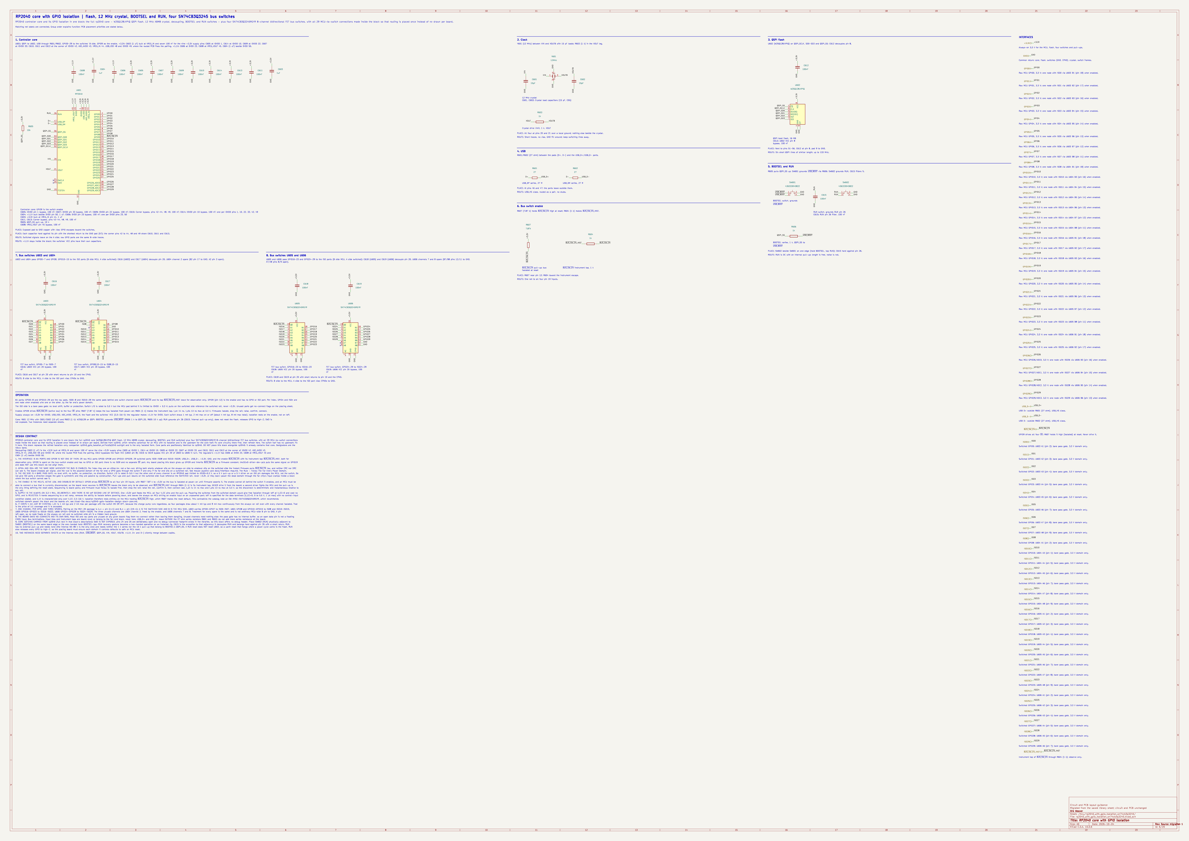
Block orb_weaver_private:rp2040_with_gpio_isolation_sn74cb3q3245 placed in /mcu of mouse-joystick-pcb. RP2040 controller core and its GPIO isolation in one block: the full rp2040 core - W25Q128JVPIQ QSPI flash, 12 MHz ABM8 crystal, decoupling, BOOTSEL and RUN switches - plus four SN74CB3Q3245RGYR 8-channel bidirectional FET bus switches, with all 29 MCU-to-switch connections made inside the block so that routing is placed once instead of re-drawn per board.
| Lifecycle | routed |
| Family | none (a private block) |
| Placement | anchor (-32, 19) mm, rotation 90°, front side |
| Sheet | rp2040_with_gpio_isolation_sn74cb3q3245.kicad_sch; sheet pins: the board's own arrangement |
| Drawing | mouse-joystick-pcb-mcu-rp2040_with_gpio_isolation_sn74cb3q3245.svg |
On the Board
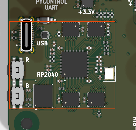
Block 9 of the board view: 28.8 × 23.7 mm on the top side, its centre 35.1 mm left of and 19.1 mm below the board centre (X right, Y up, as the enclosure tables); 35 footprints. The picture is the top render clipped around the block, the rectangle the extent of its footprints' courtyards.
Description
RP2040 controller core and its GPIO isolation in one block: the full rp2040 core (W25Q128JVPIQ QSPI flash, 12 MHz ABM8 crystal, decoupling, BOOTSEL and RUN switches) plus four SN74CB3Q3245RGYR 8-channel bidirectional FET bus switches, with all 29 MCU-to-switch connections made inside the block so that routing is placed once instead of re-drawn per board. Derived from rp2040, which remains canonical for an MCU with no isolation and is the upstream for the core half: fix core circuitry there first, then refresh here. The switch half has no upstream; fix it here. This block replaces the retired isolation-only companion rp2040_gpio_isolation_sn74cb3q3245 outright and is the only isolated form. Core parts are positionally identical to rp2040. DO NOT place this block alongside rp2040: it already contains that core. Designators are the 40xxx band. Decoupling: C40003 (1 uF) is the +3.3V bulk at VREG_IN and seven 100 nF serve the nine +3.3V supply pins: C40005 at IOVDD 1, C40014 at IOVDD 10, C40009 at IOVDD 22, C40007 at IOVDD 33, and C40010, C40011 and C40013 at the corner of IOVDD 42, ADC_AVDD 43, VREG_IN 44, USB_VDD 48 and IOVDD 49, where the routed PCB fixes the pairing. C40012 bypasses the flash VCC (U40002 pin 8); C40016 to C40019 bypass VCC pin 20 of U40003 to U40006 in turn. The regulator's +1.1V has C40006 at DVDD 23, C40008 at VREG_VOUT 45 and C40004 (1 uF) beside DVDD 50. 1. THE INTERFACE IS 64 PORTS AND GPIO9 IS NOT ONE OF THEM: 29 raw MCU ports GPIO0-GPIO8 and GPIO10-GPIO29, 29 switched ports ISO0-ISO8 and ISO10-ISO29, USB_D+, USB_D-, +3.3V, GND, and the enable ~{BUS_SW_EN} with its instrument tap ~{BUS_SW_EN}_INST, both for observation only. GPIO9 is spent on the bus-switch enable and has no GPIO or ISO port; there is no ISO9 and no separate ~{OE} port. Any board placing this block gives up GPIO9 and inherits ~{BUS_SW_EN} as a firmware constant. tmc51x0-driver-dev-pcb puts the same signal on GPIO19 and does NOT use this block; do not align them. 2. GPIOn AND ISOn ARE THE SAME NODE WHENEVER THE BUS IS ENABLED. Per index they are an either/or, not a fan-out. Wiring both shorts whatever sits on the always-on side to whatever sits on the switched side the instant firmware pulls ~{BUS_SW_EN} low, and neither ERC nor DRC can see it. The board chooses per signal, and the rule is the powered domain of the far end: a GPIO goes through the switch if and only if its far end sits on a switched rail. See mouse-joystick-pcb docs/interface-map.md, The Rule - Follow The Far End's Power Domain. 3. THE ISO SIDE IS A BARE PASS GATE: no level shift, no buffer, no protection, no direction. Switch I/O is rated 0-5.5 V but the other end of every channel is an RP2040 pad limited to IOVDD+0.3 V, so a 5 V pull-up or a 5 V driver on an ISO pin damages the MCU, not the switch. Do not give ISO ports a direction shape: the gate is symmetric and they are passive by construction. Pull-ups and pull-downs on the switched side must reference the SWITCHED rail, never +3.3V, or they back-power the dead domain through the far chip's input clamps inside a block where the bus switch cannot see it. 4. THE ENABLE IS THE MCU'S, ACTIVE LOW, AND DISABLED BY DEFAULT: GPIO9 drives ~{BUS_SW_EN} to all four pin 19 inputs, with R40007 7.87 k to +3.3V so the bus is isolated at power-on until firmware asserts it. The enable cannot sit behind the switch it enables, and an MCU must be able to connect a bus that is currently disconnected, so the board never sources it: ~{BUS_SW_EN} leaves the block only to be observed, and ~{BUS_SW_EN}_INST through R40004 (1 k) is its instrument tap. NEVER drive it from the board; a second driver fights the MCU and the pull-up is the only thing defining the reset state. Sequencing is board policy and firmware must follow it: isolate first, then drop the rail; raise the rail, confirm it, then connect last. t_en is 14 ns max and t_dis 13 ns max at 3.3 V, so the disconnect is deterministic and instantaneous relative to any rail. 5. SUPPLY IS THE ALWAYS-ON 3.3 V RAIL, DELIBERATELY, AND THERE IS NO Ioff SECOND LINE OF DEFENCE. One +3.3V port feeds the MCU, all four V_CC pins and the pull-up. Powering the switches from the switched domain would give free isolation through Ioff at V_CC=0 and cost no GPIO, and is REJECTED: it hands sequencing to a rail ramp, removes the ability to isolate before powering down, and leaves the always-on MCU driving an enable input on an unpowered part; Ioff is specified for the data terminals (V_CC=0, 0 to 5.5 V, 1 uA max) with no control-input condition stated, and V_IH is characterized only over V_CC 2.3-3.6 V. Isolation therefore rests entirely on the MCU holding ~{BUS_SW_EN} high, which R40007 makes the reset default. This contradicts the catalog note on OW-MISC-SN74CB3Q3245RGYR, which recommends switched-domain power; the block and the boards win, see kicad-libs docs/rp2040-gpio-isolation-design-block-plan.md. 6. IT COSTS 4 mA JUST BY EXISTING: I_CC is 1 mA typ and 2 mA max per package with the switch ON OR OFF, because the charge pump runs regardless, so four packages draw about 4 mA typ and 8 mA max continuously from the always-on rail even with every channel isolated. That is the price of 1:1 coverage and it is accepted. 7. ONE CHANNEL PER GPIO, AND THREE SPARES. Pairing on the RGY-20 package is A_n = pin (n+1) and B_n = pin (19-n); A IS THE SWITCHED SIDE AND B IS THE MCU SIDE. U40003 carries GPIO0-GPIO7 to ISO0-ISO7, U40004 GPIO8 and GPIO10-GPIO15 to ISO8 and ISO10-ISO15, U40005 GPIO16-GPIO23 to ISO16-ISO23, U40006 GPIO24-GPIO29 to ISO24-ISO29. The three unused channels are U40004 channel 2, freed by the enable, and U40006 channels 7 and 8. Treatment for every spare is the same and is not arbitrary: MCU-side B pin to GND, A pin left open, so no node floats on the always-on rail and no switched-side pin is a hidden hard ground. 8. THE BOARD OWES NO-CONNECTS AND ITS OWN BIAS. Most ISO and raw ports are unused on any given board; flag them no-connect rather than leaving them dangling. Unused channels need nothing else: the pass gate has no internal buffer, so an open data pin is not a floating CMOS input. Bus terminations, input bias and instrument taps are board-level or belong to the far-end block, never here. USB_D+ and USB_D- leave OUTSIDE the 27 ohm series resistors R40001 and R40002; do not add more series resistance at the board. 9. CORE GOTCHAS CARRIED FROM rp2040 (full text in that block's description): SWD IS NOT EXPOSED, pins 24 and 25 are deliberately open and no debug-connector footprint exists in the libraries, so this block offers no debug header. Place SW40002 (RUN) physically adjacent to SW40001 (BOOTSEL) on the same board edge or the one-handed hold-BOOTSEL-tap-RUN recovery gesture becomes a two-handed operation on an installed rig. C40015 is the exception to that adjacency: it decouples RUN and belongs hard against pin 26 with a short return. RUN has no external pull-up and needs none (the internal 50-80 k is the only one) and needs neither the 1 k series nor the 10 k pull-up that belong to BOOTSEL's QSPI_SS. A RUN reset does NOT reset U40002, so a warm reset that hangs where a power cycle works is the flash. RUN also releases every GPIO to high-Z, so the placing board must ensure each domain it controls defaults to safe on MCU reset. 10. TWO INSTANCES NEED SEPARATE SHEETS or the internal nets (RUN, ~{USB_BOOT}, QSPI_SS, XIN, XOUT, XOUTB, +1.1V, D+ and D-) silently merge between copies.
Ports
The brief's shape, edge, class and meaning for each port, then what the board wires it to.
| Port | Shape | Edge | Class | Wired to | Board net | Board class | GPIO | Meaning | On this board |
|---|---|---|---|---|---|---|---|---|---|
+3.3V |
passive | west | PWR_3V3_LOCAL | +3.3V_MCU |
/+3.3V_MCU |
PWR_3V3 | Always-on 3.3 V for the MCU, flash, four switches and pull-ups. | ||
GND |
passive | west | PWR_RETURN_LOCAL | GND |
/GND |
PWR_RETURN_LOCAL | Common return: core, flash, switches (GND, EPAD), crystal, switch frames. | ||
GPIO0 |
bidirectional | west | Default | PYC_UART_TX |
/PYC_UART_TX |
MCU_FINE | GP0 |
Raw MCU GPIO0, 3.3 V; one node with ISO0 via U40003 B1 (pin 18) when enabled. | UART TX to pyControl (UART0 TX); out as the MCU sees it |
GPIO1 |
bidirectional | west | Default | PYC_UART_RX |
/PYC_UART_RX |
MCU_FINE | GP1 |
Raw MCU GPIO1, 3.3 V; one node with ISO1 via U40003 B2 (pin 17) when enabled. | UART RX from pyControl (UART0 RX); in as the MCU sees it |
GPIO2 |
bidirectional | west | Default | open: no-connect flag | Raw MCU GPIO2, 3.3 V; one node with ISO2 via U40003 B3 (pin 16) when enabled. | ||||
GPIO3 |
bidirectional | west | Default | open: no-connect flag | Raw MCU GPIO3, 3.3 V; one node with ISO3 via U40003 B4 (pin 15) when enabled. | ||||
GPIO4 |
bidirectional | west | Default | open: no-connect flag | Raw MCU GPIO4, 3.3 V; one node with ISO4 via U40003 B5 (pin 14) when enabled. | ||||
GPIO5 |
bidirectional | west | Default | open: no-connect flag | Raw MCU GPIO5, 3.3 V; one node with ISO5 via U40003 B6 (pin 13) when enabled. | ||||
GPIO6 |
bidirectional | west | Default | open: no-connect flag | Raw MCU GPIO6, 3.3 V; one node with ISO6 via U40003 B7 (pin 12) when enabled. | ||||
GPIO7 |
bidirectional | west | Default | open: no-connect flag | Raw MCU GPIO7, 3.3 V; one node with ISO7 via U40003 B8 (pin 11) when enabled. | ||||
GPIO8 |
bidirectional | west | Default | open: no-connect flag | Raw MCU GPIO8, 3.3 V; one node with ISO8 via U40004 B1 (pin 18) when enabled. | ||||
GPIO10 |
bidirectional | west | Default | open: no-connect flag | Raw MCU GPIO10, 3.3 V; one node with ISO10 via U40004 B3 (pin 16) when enabled. | ||||
GPIO11 |
bidirectional | west | Default | open: no-connect flag | Raw MCU GPIO11, 3.3 V; one node with ISO11 via U40004 B4 (pin 15) when enabled. | ||||
GPIO12 |
bidirectional | west | Default | open: no-connect flag | Raw MCU GPIO12, 3.3 V; one node with ISO12 via U40004 B5 (pin 14) when enabled. | ||||
GPIO13 |
bidirectional | west | Default | open: no-connect flag | Raw MCU GPIO13, 3.3 V; one node with ISO13 via U40004 B6 (pin 13) when enabled. | ||||
GPIO14 |
bidirectional | west | Default | HV_DIAG_EN |
/HV_DIAG_EN |
MCU_FINE | GP14 |
Raw MCU GPIO14, 3.3 V; one node with ISO14 via U40004 B7 (pin 12) when enabled. | 36 V switch diagnostics enable⁵; out as the MCU sees it |
GPIO15 |
bidirectional | west | Default | open: no-connect flag | Raw MCU GPIO15, 3.3 V; one node with ISO15 via U40004 B8 (pin 11) when enabled. | ||||
GPIO16 |
bidirectional | west | Default | DAC_SDA_BYP |
/mcu/DAC_SDA_BYP |
MCU_FINE | Raw MCU GPIO16, 3.3 V; one node with ISO16 via U40005 B1 (pin 18) when enabled. | ||
GPIO17 |
bidirectional | west | Default | DAC_SCL_BYP |
/mcu/DAC_SCL_BYP |
MCU_FINE | Raw MCU GPIO17, 3.3 V; one node with ISO17 via U40005 B2 (pin 17) when enabled. | ||
GPIO18 |
bidirectional | west | Default | open: no-connect flag | Raw MCU GPIO18, 3.3 V; one node with ISO18 via U40005 B3 (pin 16) when enabled. | ||||
GPIO19 |
bidirectional | west | Default | HV_EN |
/HV_EN |
MCU_FINE | GP19 |
Raw MCU GPIO19, 3.3 V; one node with ISO19 via U40005 B4 (pin 15) when enabled. | 36 V input switch enable; out as the MCU sees it |
GPIO20 |
bidirectional | west | Default | open: no-connect flag | Raw MCU GPIO20, 3.3 V; one node with ISO20 via U40005 B5 (pin 14) when enabled. | ||||
GPIO21 |
bidirectional | west | Default | FW_TRIG1 |
/FW_TRIG1 |
MCU_FINE | GP21 |
Raw MCU GPIO21, 3.3 V; one node with ISO21 via U40005 B6 (pin 13) when enabled. | Firmware timing marker; out as the MCU sees it |
GPIO22 |
bidirectional | west | Default | open: no-connect flag | Raw MCU GPIO22, 3.3 V; one node with ISO22 via U40005 B7 (pin 12) when enabled. | ||||
GPIO23 |
bidirectional | west | Default | ~{HV_FAULT} |
/~{HV_FAULT} |
MCU_FINE | GP23 |
Raw MCU GPIO23, 3.3 V; one node with ISO23 via U40005 B8 (pin 11) when enabled. | 36 V switch fault, open-drain, pull-up 3.3 V¹¹; in as the MCU sees it |
GPIO24 |
bidirectional | west | Default | HV_LATCH |
/HV_LATCH |
MCU_FINE | GP24 |
Raw MCU GPIO24, 3.3 V; one node with ISO24 via U40006 B1 (pin 18) when enabled. | 36 V switch latch-off select¹⁰; out as the MCU sees it |
GPIO25 |
bidirectional | west | Default | FW_TRIG0 |
/FW_TRIG0 |
MCU_FINE | GP25 |
Raw MCU GPIO25, 3.3 V; one node with ISO25 via U40006 B2 (pin 17) when enabled. | Firmware timing marker; out as the MCU sees it |
GPIO26 |
passive | west | Default | SW_RAIL_SENSE_DIV_2 |
/mcu/SW_RAIL_SENSE_DIV_2 |
MCU_FINE | GP26 |
Raw MCU GPIO26/ADC0, 3.3 V; one node with ISO26 via U40006 B3 (pin 16) when enabled. | +3.3V_SW presence and level, divided by 2 inside mcu (R408/R409); in as the MCU sees it |
GPIO27 |
passive | west | Default | BRAKE_ISENSE |
/BRAKE_ISENSE |
MCU_FINE | GP27 |
Raw MCU GPIO27/ADC1, 3.3 V; one node with ISO27 via U40006 B4 (pin 15) when enabled. | Brake sink current readback, ADC1¹¹; in as the MCU sees it |
GPIO28 |
passive | west | Default | HV_SNS |
/HV_SNS |
MCU_FINE | GP28 |
Raw MCU GPIO28/ADC2, 3.3 V; one node with ISO28 via U40006 B5 (pin 14) when enabled. | 36 V input load-current sense, R_SNS = 249 Ω; in as the MCU sees it |
GPIO29 |
passive | west | Default | ANGLE_OUT_MON |
/ANGLE_OUT_MON |
MCU_FINE | GP29 |
Raw MCU GPIO29/ADC3, 3.3 V; one node with ISO29 via U40006 B6 (pin 13) when enabled. | Analog output readback, ADC3¹¹; in as the MCU sees it |
ISO0 |
passive | east | Default | open: no-connect flag | Switched GPIO0: U40003 A1 (pin 2); bare pass gate, 3.3 V domain only. | ||||
ISO1 |
passive | east | Default | open: no-connect flag | Switched GPIO1: U40003 A2 (pin 3); bare pass gate, 3.3 V domain only. | ||||
ISO2 |
passive | east | Default | ~{TMC_CS} |
/~{TMC_CS} |
Default | GP2 |
Switched GPIO2: U40003 A3 (pin 4); bare pass gate, 3.3 V domain only. | Driver chip select; out as the MCU sees it, via the bus switch |
ISO3 |
passive | east | Default | ~{TMC_DRV_EN} |
/~{TMC_DRV_EN} |
Default | GP3 |
Switched GPIO3: U40003 A4 (pin 5); bare pass gate, 3.3 V domain only. | Driver enable, active low; out as the MCU sees it, via the bus switch |
ISO4 |
passive | east | Default | TMC_SPI_CIPO |
/TMC_SPI_CIPO |
Default | GP4 |
Switched GPIO4: U40003 A5 (pin 6); bare pass gate, 3.3 V domain only. | Driver SPI CIPO (SPI0 RX); in as the MCU sees it, via the bus switch |
ISO5 |
passive | east | Default | TMC_DIAG0 |
/TMC_DIAG0 |
Default | GP5 |
Switched GPIO5: U40003 A6 (pin 7); bare pass gate, 3.3 V domain only. | Driver diagnostic 0; in as the MCU sees it, via the bus switch |
ISO6 |
passive | east | Default | TMC_SPI_SCK |
/TMC_SPI_SCK |
Default | GP6 |
Switched GPIO6: U40003 A7 (pin 8); bare pass gate, 3.3 V domain only. | Driver SPI clock (SPI0 SCK); out as the MCU sees it, via the bus switch |
ISO7 |
passive | east | Default | TMC_SPI_COPI |
/TMC_SPI_COPI |
Default | GP7 |
Switched GPIO7: U40003 A8 (pin 9); bare pass gate, 3.3 V domain only. | Driver SPI COPI (SPI0 TX); out as the MCU sees it, via the bus switch |
ISO8 |
passive | east | Default | TMC_DIAG1 |
/TMC_DIAG1 |
Default | GP8 |
Switched GPIO8: U40004 A1 (pin 2); bare pass gate, 3.3 V domain only. | Driver diagnostic 1; in as the MCU sees it, via the bus switch |
ISO10 |
passive | east | Default | TQ_SPI_SCK |
/TQ_SPI_SCK |
Default | GP10 |
Switched GPIO10: U40004 A3 (pin 4); bare pass gate, 3.3 V domain only. | Torque ADC SPI clock (SPI1 SCK)⁷; out as the MCU sees it, via the bus switch |
ISO11 |
passive | east | Default | TQ_SPI_COPI |
/TQ_SPI_COPI |
Default | GP11 |
Switched GPIO11: U40004 A4 (pin 5); bare pass gate, 3.3 V domain only. | Torque ADC SPI COPI (SPI1 TX)⁷; out as the MCU sees it, via the bus switch |
ISO12 |
passive | east | Default | TQ_SPI_CIPO |
/TQ_SPI_CIPO |
Default | GP12 |
Switched GPIO12: U40004 A5 (pin 6); bare pass gate, 3.3 V domain only. | Torque ADC SPI CIPO (SPI1 RX)⁷; in as the MCU sees it, via the bus switch |
ISO13 |
passive | east | Default | ~{BRAKE_FAULT} |
/~{BRAKE_FAULT} |
Default | GP13 |
Switched GPIO13: U40004 A6 (pin 7); bare pass gate, 3.3 V domain only. | Brake block fault, active low⁷; in as the MCU sees it, via the bus switch |
ISO14 |
passive | east | Default | open: no-connect flag | Switched GPIO14: U40004 A7 (pin 8); bare pass gate, 3.3 V domain only. | ||||
ISO15 |
passive | east | Default | TQ_CONVST_CS |
/TQ_CONVST_CS |
Default | GP15 |
Switched GPIO15: U40004 A8 (pin 9); bare pass gate, 3.3 V domain only. | ADS8689 convert-start / frame, plain GPIO⁷; out as the MCU sees it, via the bus switch |
ISO16 |
passive | east | Default | DAC_SDA |
/DAC_SDA |
Default | GP16 |
Switched GPIO16: U40005 A1 (pin 2); bare pass gate, 3.3 V domain only. | I2C0 SDA — analog 0x48, brake 0x49⁷; bidi as the MCU sees it, via the bus switch |
ISO17 |
passive | east | Default | DAC_SCL |
/DAC_SCL |
Default | GP17 |
Switched GPIO17: U40005 A2 (pin 3); bare pass gate, 3.3 V domain only. | I2C0 SCL — same bus⁷; out as the MCU sees it, via the bus switch |
ISO18 |
passive | east | Default | TQ_CAL_EN |
/TQ_CAL_EN |
Default | GP18 |
Switched GPIO18: U40005 A3 (pin 4); bare pass gate, 3.3 V domain only. | Torque calibration enable⁷; out as the MCU sees it, via the bus switch |
ISO19 |
passive | east | Default | open: no-connect flag | Switched GPIO19: U40005 A4 (pin 5); bare pass gate, 3.3 V domain only. | ||||
ISO20 |
passive | east | Default | open: no-connect flag | Switched GPIO20: U40005 A5 (pin 6); bare pass gate, 3.3 V domain only. | ||||
ISO21 |
passive | east | Default | open: no-connect flag | Switched GPIO21: U40005 A6 (pin 7); bare pass gate, 3.3 V domain only. | ||||
ISO22 |
passive | east | Default | open: no-connect flag | Switched GPIO22: U40005 A7 (pin 8); bare pass gate, 3.3 V domain only. | ||||
ISO23 |
passive | east | Default | open: no-connect flag | Switched GPIO23: U40005 A8 (pin 9); bare pass gate, 3.3 V domain only. | ||||
ISO24 |
passive | east | Default | open: no-connect flag | Switched GPIO24: U40006 A1 (pin 2); bare pass gate, 3.3 V domain only. | ||||
ISO25 |
passive | east | Default | open: no-connect flag | Switched GPIO25: U40006 A2 (pin 3); bare pass gate, 3.3 V domain only. | ||||
ISO26 |
passive | east | Default | open: no-connect flag | Switched GPIO26: U40006 A3 (pin 4); bare pass gate, 3.3 V domain only. | ||||
ISO27 |
passive | east | Default | open: no-connect flag | Switched GPIO27: U40006 A4 (pin 5); bare pass gate, 3.3 V domain only. | ||||
ISO28 |
passive | east | Default | open: no-connect flag | Switched GPIO28: U40006 A5 (pin 6); bare pass gate, 3.3 V domain only. | ||||
ISO29 |
passive | east | Default | open: no-connect flag | Switched GPIO29: U40006 A6 (pin 7); bare pass gate, 3.3 V domain only. | ||||
USB_D+ |
bidirectional | west | USB_HS | USB_D+ |
/USB_D+ |
USB_HS | USB D+ outside R40001 (27 ohm), USB_HS class. | ||
USB_D- |
bidirectional | west | USB_HS | USB_D- |
/USB_D- |
USB_HS | USB D- outside R40002 (27 ohm), USB_HS class. | ||
~{BUS_SW_EN} |
output | west | Default | open: no-connect flag | GPIO9 drives all four ~{OE}; R40007 holds it high (isolated) at reset. Never drive it. | ||||
~{BUS_SW_EN}_INST |
output | east | INSTRUMENT | ~{BUS_SW_EN}_INST |
/~{BUS_SW_EN}_INST |
INSTRUMENT | Instrument tap of ~{BUS_SW_EN} through R40004 (1 k); observe only. |
Parts
As placed on the board's sheet; 35 of 35 paired with the brief's references by symbol identity, the rest given the brief's role where the internal part has one, else the catalog's role slug; the placement is the Placement field of the board's symbol, else of the library's (D38); the manufacturer part and the LCSC number are the board's BOM's.
| Reference | Brief | Part | Value | Role | Placement | Manufacturer part | LCSC | DNP |
|---|---|---|---|---|---|---|---|---|
C601 |
C40001 |
OW-PASS-C0402C150J3GACAUTO |
15pF | Crystal load capacitors (15 pF, C0G) | beside Y601.1, on XIN | C0402C150J3GACAUTO | C3888936 | |
C602 |
C40002 |
OW-PASS-C0402C150J3GACAUTO |
15pF | Crystal load capacitors (15 pF, C0G) | beside Y601.3, on XOUTB | C0402C150J3GACAUTO | C3888936 | |
C603 |
C40003 |
OW-PASS-CL05A105KL5NRNC |
1uF | +3.3V bulk at VREG_IN pin 44, 1 uF | beside U601.44 (VREG_IN), on +3.3V | CL05A105KL5NRNC | C307413 | |
C604 |
C40004 |
OW-PASS-CL05A105KL5NRNC |
1uF | +1.1V bulk beside DVDD pin 50, 1 uF | beside U601 DVDD pins 23, 50 (one per pin), on +1.1V | CL05A105KL5NRNC | C307413 | |
C605 |
C40005 |
OW-CAP-100N-0402-X5R-16V |
100nF | IOVDD pin 1 bypass, 100 nF | beside U601 IOVDD pins 1, 10, 22, 33, 42, 49 (one per pin), on +3.3V | GRM155R62A104KE14D | C162178 | |
C606 |
C40006 |
OW-CAP-100N-0402-X5R-16V |
100nF | DVDD pin 23 bypass, 100 nF | beside U601 DVDD pins 23, 50 (one per pin), on +1.1V | GRM155R62A104KE14D | C162178 | |
C607 |
C40007 |
OW-CAP-100N-0402-X5R-16V |
100nF | IOVDD pin 33 bypass, 100 nF | beside U601 IOVDD pins 1, 10, 22, 33, 42, 49 (one per pin), on +3.3V | GRM155R62A104KE14D | C162178 | |
C608 |
C40008 |
OW-CAP-100N-0402-X5R-16V |
100nF | VREG_VOUT pin 45 bypass, 100 nF | beside U601.45 (VREG_VOUT), on +1.1V | GRM155R62A104KE14D | C162178 | |
C609 |
C40009 |
OW-CAP-100N-0402-X5R-16V |
100nF | IOVDD pin 22 bypass, 100 nF | beside U601 IOVDD pins 1, 10, 22, 33, 42, 49 (one per pin), on +3.3V | GRM155R62A104KE14D | C162178 | |
C610 |
C40010 |
OW-CAP-100N-0402-X5R-16V |
100nF | Corner bypass, pins 42-44, 48, 49, 100 nF | beside U601 IOVDD pins 1, 10, 22, 33, 42, 49 (one per pin), on +3.3V | GRM155R62A104KE14D | C162178 | |
C611 |
C40011 |
OW-CAP-100N-0402-X5R-16V |
100nF | Corner bypass, pins 42-44, 48, 49, 100 nF | beside U601.43 (ADC_AVDD), on +3.3V | GRM155R62A104KE14D | C162178 | |
C612 |
C40012 |
OW-CAP-100N-0402-X5R-16V |
100nF | U40002 VCC pin 8 bypass, 100 nF | beside U602.8 (VCC), on +3.3V | GRM155R62A104KE14D | C162178 | |
C613 |
C40013 |
OW-CAP-100N-0402-X5R-16V |
100nF | Corner bypass, pins 42-44, 48, 49, 100 nF | beside U601.48 (USB_VDD), on +3.3V | GRM155R62A104KE14D | C162178 | |
C614 |
C40014 |
OW-CAP-100N-0402-X5R-16V |
100nF | IOVDD pin 10 bypass, 100 nF | beside U601 IOVDD pins 1, 10, 22, 33, 42, 49 (one per pin), on +3.3V | GRM155R62A104KE14D | C162178 | |
C615 |
C40015 |
OW-CAP-100N-0402-X5R-16V |
100nF | RUN pin 26 filter, 100 nF | beside SW602.1, on RUN | GRM155R62A104KE14D | C162178 | |
C616 |
C40016 |
OW-CAP-100N-0402-X5R-16V |
100nF | U40003 VCC pin 20 bypass, 100 nF | beside U603.20 (VCC), on +3.3V | GRM155R62A104KE14D | C162178 | |
C617 |
C40017 |
OW-CAP-100N-0402-X5R-16V |
100nF | U40004 VCC pin 20 bypass, 100 nF | beside U604.20 (VCC), on +3.3V | GRM155R62A104KE14D | C162178 | |
C618 |
C40018 |
OW-CAP-100N-0402-X5R-16V |
100nF | U40005 VCC pin 20 bypass, 100 nF | beside U605.20 (VCC), on +3.3V | GRM155R62A104KE14D | C162178 | |
C619 |
C40019 |
OW-CAP-100N-0402-X5R-16V |
100nF | U40006 VCC pin 20 bypass, 100 nF | beside U606.20 (VCC), on +3.3V | GRM155R62A104KE14D | C162178 | |
R601 |
R40001 |
OW-RES-27R-0402 |
27 | USB_DP series, 27 R | ERJ2GEJ270X | C278580 | ||
R602 |
R40002 |
OW-RES-27R-0402 |
27 | USB_DM series, 27 R | ERJ2GEJ270X | C278580 | ||
R603 |
R40003 |
OW-PASS-RC0402FR-071KL |
1k | Crystal drive limit, 1 k, XOUT | RC0402FR-071KL | C106235 | ||
R604 |
R40004 |
OW-PASS-RC0402FR-071KL |
1k | ~{BUS_SW_EN} instrument tap, 1 k | RC0402FR-071KL | C106235 | ||
R605 |
R40005 |
OW-RES-10K-0402 |
10k | QSPI_SS pull-up, 10 k | beside U601.56 (QSPI_SS), on QSPI_SS | ERJ2GEJ103X | C278577 | |
R606 |
R40006 |
OW-PASS-RC0402FR-071KL |
1k | BOOTSEL series, 1 k, QSPI_SS to ~{USB_BOOT} | RC0402FR-071KL | C106235 | ||
R607 |
R40007 |
OW-PASS-FRC0402F7871TS |
7.87k | ~{BUS_SW_EN} pull-up: bus isolated at reset | FRC0402F7871TS | C2998145 | ||
SW601 |
SW40001 |
OW-MISC-436333045822 |
436333045822 | BOOTSEL switch, grounds ~{USB_BOOT} | 436333045822 | C7185056 | ||
SW602 |
SW40002 |
OW-MISC-436333045822 |
436333045822 | RUN switch, grounds RUN pin 26 | 436333045822 | C7185056 | ||
U601 |
U40001 |
OW-MCU-RP2040 |
RP2040 | Controller core; GPIO9 is the switch enable | RP2040 | C2040 | ||
U602 |
U40002 |
OW-MCU-W25Q128JVPIQ |
W25Q128JVPIQ | QSPI boot flash, 16 MB | W25Q128JVPIQ | C190862 | ||
U603 |
U40003 |
OW-MISC-SN74CB3Q3245RGYR |
SN74CB3Q3245RGYR | FET bus switch, GPIO0-7 to ISO0-7 | SN74CB3Q3245RGYR | C201559 | ||
U604 |
U40004 |
OW-MISC-SN74CB3Q3245RGYR |
SN74CB3Q3245RGYR | FET bus switch, GPIO8,10-15 to ISO8,10-15 | SN74CB3Q3245RGYR | C201559 | ||
U605 |
U40005 |
OW-MISC-SN74CB3Q3245RGYR |
SN74CB3Q3245RGYR | FET bus switch, GPIO16-23 to ISO16-23 | SN74CB3Q3245RGYR | C201559 | ||
U606 |
U40006 |
OW-MISC-SN74CB3Q3245RGYR |
SN74CB3Q3245RGYR | FET bus switch, GPIO24-29 to ISO24-29 | SN74CB3Q3245RGYR | C201559 | ||
Y601 |
Y40001 |
OW-XTAL-12M-3225-10PF |
12MHz | 12 MHz crystal | ABM8-272-T3 | C20625731 |
Operating Notes
- 64 ports: GPIO0-8 and GPIO10-29 are the raw pads, ISO0-8 and ISO10-29 the same pads behind one switch channel each; ~{BUS_SW_EN} and its tap ~{BUS_SW_EN}_INST leave for observation only. GPIO9 (pin 12) is the enable and has no GPIO or ISO port. Per index, GPIOn and ISOn are one node when enabled: wire one or the other, by the far end's power domain.
- The ISO side is a bare pass gate: no level shift, buffer or protection. Switch I/O is rated to 5.5 V but the MCU pad behind it is limited to IOVDD + 0.3 V; pulls on the switched side reference the switched rail, never +3.3V. Unused ports get no-connect flags on the placing sheet.
- Enable: GPIO9 drives ~{BUS_SW_EN} (active low) to the four ~{OE} pins; R40007 (7.87 k) keeps the bus isolated from power-on; R40004 (1 k) makes the instrument tap. t_en 14 ns, t_dis 13 ns max at 3.3 V. Firmware: isolate, drop the rail; raise, confirm, connect.
- Supply: always-on +3.3V for IOVDD, USB_VDD, ADC_AVDD, VREG_IN, the flash and the switches' VCC (2.3-3.6 V); the regulator makes +1.1V for DVDD. Each switch draws 1 mA typ, 2 mA max on or off (about 4 mA typ, 8 mA max total). Isolation rests on the enable, not on Ioff.
- Core: Y40001 12 MHz with C40001/C40002 (15 pF) and R40003 (1 k); W25Q128 on QSPI; BOOTSEL grounds ~{USB_BOOT} (R40006 1 k to QSPI_SS, R40005 10 k up); RUN grounds pin 26 (C40015, internal pull-up only), does not reset the flash, releases GPIO to high-Z. SWD is not exposed. Two instances need separate sheets.
Placement and Routing
Controller core
U40001, C40003, C40005, C40007, C40009, C40010, C40011, C40013, C40014, R40005, C40004, C40006, C40008
U40001: QSPI to U40002, USB through R40001/R40002, GPIO0-29 to the switches' B side, GPIO9 as the enable. +3.3V: C40003 (1 uF) bulk at VREG_IN and seven 100 nF for the nine +3.3V supply pins: C40005 at IOVDD 1, C40014 at IOVDD 10, C40009 at IOVDD 22, C40007 at IOVDD 33; C40010, C40011 and C40013 at the corner of IOVDD 42, ADC_AVDD 43, VREG_IN 44, USB_VDD 48 and IOVDD 49, where the routed PCB fixes the pairing. +1.1V: C40006 at DVDD 23, C40008 at VREG_VOUT 45, C40004 (1 uF) beside DVDD 50.
- Place: Exposed pad to GND copper with vias; GPIO escapes toward the switches.
- Place: Each capacitor hard against its pin with the shortest return to the GND pad (57); the corner pins 42 to 44, 48 and 49 share C40010, C40011 and C40013.
- Route: Switched signals leave on the A side; raw GPIO ports are the same B-side traces.
- Route: +1.1V stays inside the block; the switches' VCC pins have their own capacitors.
Clock
C40001, Y40001, C40002, R40003
Y40001 (12 MHz) between XIN and XOUTB with 15 pF loads; R40003 (1 k) in the XOUT leg.
- Place: All four at pins 20 and 21 over a local ground; nothing else beside the crystal.
- Route: Short traces, no vias, GND fill around; keep switching lines away.
QSPI flash
U40002, C40012
U40002 (W25Q128JVPIQ) on QSPI_SCLK, SD0-SD3 and QSPI_SS; C40012 decouples pin 8.
- Place: Next to pins 51-56, C40012 at pin 8, pad 9 to GND.
- Route: Six short QSPI lines of similar length; up to 133 MHz.
USB
R40001, R40002
R40001/R40002 (27 ohm) between the pads (D+, D-) and the USB_D+/USB_D- ports.
- Place: At pins 46 and 47; the ports leave outside them.
- Route: USB_HS class, routed as a pair, no stubs.
BOOTSEL and RUN
R40006, SW40001, SW40002, C40015
R40005 pulls QSPI_SS up; SW40001 grounds ~{USB_BOOT} via R40006; SW40002 grounds RUN, C40015 filters it.
- Place: SW40002 beside SW40001 on one edge (hold BOOTSEL, tap RUN); C40015 hard against pin 26.
- Route: RUN is DC with an internal pull-up: length is free, noise is not.
Bus switch enable
R40007, R40004
R40007 (7.87 k) holds ~{BUS_SW_EN} high at reset; R40004 (1 k) makes ~{BUS_SW_EN}_INST.
- Place: R40007 near pin 12; R40004 toward the instrument escape.
- Route: One net to all four pin 19 inputs.
Bus switches U40003 and U40004
U40003, C40016, U40004, C40017
U40003 and U40004 pass GPIO0-7 and GPIO8, GPIO10-15 to the ISO ports (B side MCU, A side switched); C40016 (U40003) and C40017 (U40004) decouple pin 20. U40004 channel 2 spare (B2 pin 17 to GND, A2 pin 3 open).
- Place: C40016 and C40017 at pin 20 with short returns to pin 10 and the EPAD.
- Route: B side to the MCU, A side to the ISO port vias; EPADs to GND.
Bus switches U40005 and U40006
U40005, C40018, U40006, C40019
U40005 and U40006 pass GPIO16-23 and GPIO24-29 to the ISO ports (B side MCU, A side switched); C40018 (U40005) and C40019 (U40006) decouple pin 20. U40006 channels 7 and 8 spare (B7/B8 pins 12/11 to GND, A7/A8 pins 8/9 open).
- Place: C40018 and C40019 at pin 20 with short returns to pin 10 and the EPAD.
- Route: B side to the MCU, A side to the ISO port vias; EPADs to GND.
Library Identity
| Block | orb_weaver_private:rp2040_with_gpio_isolation_sn74cb3q3245 |
| Resolution | the placed id is in the library |
| Brief | design_blocks/orb_weaver_private.kicad_blocks/rp2040_with_gpio_isolation_sn74cb3q3245.kicad_block/rp2040_with_gpio_isolation_sn74cb3q3245.brief.yaml, the block's brief |
| Published sheet | 8ead76fd0ae4e22c |
| Published PCB | d79a8f4d7e226204 |
| Source lock | symbol snapshot 43790a2d8bf6787f, published 2026-10-14 |
| Placed sheet | 740f29d1bb57716a: matches the brief: its 35 parts by internal part, every port by name and shape; the file is the board's copy under its own designators |
| Netlist check | ok on 2026-10-15: every pin on the brief's net; 40 identity records differ, the board's own instances |