pycontrol_behavior_port_rj45_boundary_vertical
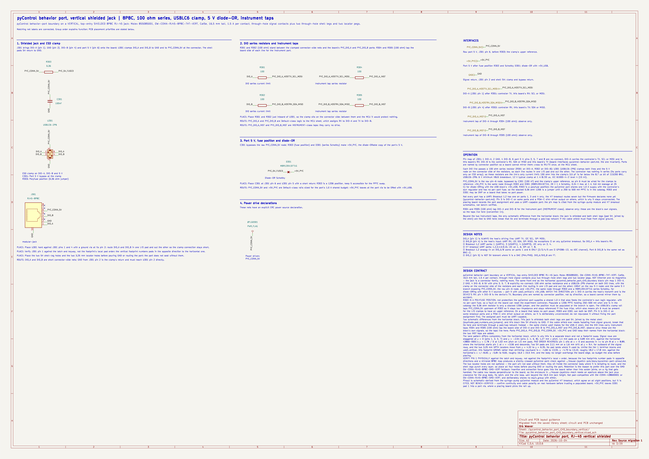
Block orb_weaver_private:pycontrol_behavior_port_rj45_boundary_vertical placed in / of mouse-joystick-pcb. pyControl behavior-port boundary on a VERTICAL, top-entry SHIELDED 8P8C RJ-45 jack: Molex 855085001, OW-CONN-RJ45-8P8C-THT-VERT, Cat5e, 16.5 mm tall, 1.5 A per contact, through-hole signal contacts plus two through-hole shell legs and two locator pegs.
| Lifecycle | routed |
| Family | none (a private block) |
| Placement | anchor (-39.98, -8) mm, rotation 270°, front side; as built: -39.98, -8 is off the 1 mm grid (review) |
| Sheet | pycontrol_behavior_port_rj45_boundary_vertical.kicad_sch; sheet pins: the board's own arrangement |
| Drawing | mouse-joystick-pcb-pycontrol_behavior_port_rj45_boundary_vertical.svg |
On the Board

Block 5 of the board view: 23.2 × 17.0 mm on the top side, its centre 38.4 mm left of and 8.0 mm above the board centre (X right, Y up, as the enclosure tables); 9 footprints. The picture is the top render clipped around the block, the rectangle the extent of its footprints' courtyards.
Description
pyControl behavior-port boundary on a VERTICAL, top-entry SHIELDED 8P8C RJ-45 jack: Molex 855085001, OW-CONN-RJ45-8P8C-THT-VERT, Cat5e, 16.5 mm tall, 1.5 A per contact, through-hole signal contacts plus two through-hole shell legs and two locator pegs. NOT Ethernet and no magnetics — the jack is a connector family, nothing more. The same front end as the horizontal pycontrol_behavior_port_rj45_boundary block: pin map 1 DIO-A, 2 GND, 4 DIO-B, 6 5V with pins 3, 5, 7, 8 explicitly no-connect; 100 ohm series resistance and a USBLC6-2P6 channel on both DIO lines, with the clamp on the connector side of the resistors and each line routing in one I/O pad and out the other; 100nF on the raw 5 V node; and the same 5 V branch exposing PYC_CONN_5V, the raw pin-6 node, and +5V_PYC, the same node through R32003 and a MBR120VLSFT1G series Schottky, for diode-ORing with other 5 V sources — pair it with usb2_vertical's +5V_USB. WATCH THE DIRECTION: pin 1 DIO-A carries the host's transmit and is the DEVICE'S RX; pin 4 DIO-B is the device's TX. Boundary pins are named by connector position, not by direction, so a board cannot mirror them by accident. R32003 IS A POLYFUSE POSITION, not protection: the pyControl port supplies a shared 1.0 A that also feeds the controller's own logic regulator, with no per-port fuse, so a fault on the board can reset the experiment controller. Populate a 1206 PPTC holding 250-500 mA when one is in the catalog; the 0.36 ohm resistor is only a stocked 1206 jumper, and the position must be populated or the branch is open. The USBLC6's clamp rail taps PYC_CONN_5V upstream of R32003 so it stays low-impedance and stays referenced if the fuse trips, which also means pin 6 must be present for the I/O clamps to have an upper reference. On a board that takes no port power, R32003 and D32001 can both be DNP. Pin 5 is DIO-C on some breakout ports and a POW-C sink driver output on others, so it is deliberately unconnected; do not repurpose it without fixing the port assignment first. The assigned port must be UART-capable. Two schematic differences from the horizontal block. This jack is shielded: both shell legs are pad SH, joined by the metal shell (duplicate_pad_numbers_are_jumpers), and this block ties SH directly to GND. If the cable shield ever needs isolating from signal ground, break that tie here and terminate through a pad/cap network instead — the same choice usb2 makes for the USB-C shell. And the DIO lines carry instrument taps: R32004 and R32005 (100 ohm) tap the board side of DIO-A and DIO-B to PYC_DIO_A_INST and PYC_DIO_B_INST, observe only; these are the block's own signals, so the taps live here. Ports PYC_DIO_A, PYC_DIO_B, PYC_CONN_5V, +5V_PYC and GND keep their names from the horizontal block; the two INST taps are added. The land pattern differs completely from the horizontal block, which is why this is a separate block and not a footprint swap. Signal rows are staggered at y = 0 (pins 1, 3, 5, 7) and y = -2.54 (pins 2, 4, 6, 8), 1.27 mm x pitch, 1.4 mm pads on a 0.89 mm drill, against the horizontal 43860-0001's y = 1.78 / 0 at 1.02 mm pitch on 1.5 mm pads. PAD ORDER REVERSES: pin 1 sits at x = 0 and ascends in +x to pin 8 at x = 8.89, where the horizontal starts pin 1 at x = +3.56 and descends. Two SH pads are 2.11 mm on a 1.6 mm drill at y = 9.4, far outboard of the signal rows, and the two 3.25 mm NPTH locators move from y = 4.32 to y = 6.35. No pad lands where it used to. Unlike the tier 1 terminal blocks and usb2_vertical, this footprint GROWS rather than shrinking: courtyard is x -4.66 to 13.55, y -4.70 to 13.10, roughly 18.2 x 17.8 mm, against the horizontal's x +/-8.00, y -5.84 to 9.65, roughly 16.0 x 15.5 mm, and the body no longer overhangs the board edge, so budget the area before placing. VERIFY PIN 1 PHYSICALLY against the latch and keyway, not against the footprint's local x order, because the two footprints number pads in opposite directions and a mirrored 8P8C map produces a silently crossed pyControl port; check against ../mouse-joystick-pcb/docs/pycontrol-port-pinout.md. The two locator holes are not optional — the part will not seat without them, they sit inside the connector body where it is tempting to route, and the shell legs punch every layer, so place all four holes before pouring GND or routing the port. Retention is the reason to prefer this part over the SMD OW-CONN-RJ45-8P8C-SMD-VERT fallback: insertion and extraction force goes into the board rather than into solder joints, on a rig that gets handled. The cable now leaves perpendicular to the board, so the enclosure in ../mouse-joysticks-mech needs an aperture above the jack plus clearance for the plug body, its latch, and the wire loop, well beyond the 16.5 mm jack height. Not pad-compatible with OW-CONN-438600001 or OW-CONN-RJ45-8P8C-SMD-VERT, and deliberately shares no equiv_group with either. Pinout is schematic-derived from the syringe-pump pyControl module and the pyControl H7 breakout, which agree on all eight positions, but it is CITED, NOT BENCH-VERIFIED — confirm continuity and cable polarity on real hardware before trusting a populated board. +5V_PYC leaves D32001 pad 1 into a port via, where a placing board picks the rail up.
Ports
The brief's shape, edge, class and meaning for each port, then what the board wires it to.
| Port | Shape | Edge | Class | Wired to | Board net | Board class | GPIO | Meaning | On this board |
|---|---|---|---|---|---|---|---|---|---|
+5V_PYC |
passive | east | Default | +5V_MCU |
/+5V_MCU |
PWR_5V | Port 5 V after fuse position R32003 and Schottky D32001; diode-OR with +5V_USB. | ||
GND |
passive | east | PWR_RETURN_LOCAL | GND |
/GND |
PWR_RETURN_LOCAL | Signal return, J32001 pin 2 and shell SH; clamp and bypass return. | ||
PYC_CONN_5V |
passive | east | Default | open: no-connect flag | Raw port 5 V, J32001 pin 6, before R32003; the clamp's upper reference. | ||||
PYC_DIO_A_HOSTTX_SCL_MOSI |
bidirectional | east | Default | PYC_UART_RX |
/PYC_UART_RX |
MCU_FINE | GP1 |
DIO-A (J32001 pin 1) after R32001: controller TX, this board's RX; SCL or MOSI. | UART RX from pyControl (UART0 RX); in as the MCU sees it |
PYC_DIO_A_INST |
output | east | INSTRUMENT | PYC_UART_RX_INST |
/PYC_UART_RX_INST |
INSTRUMENT | Instrument tap of DIO-A through R32004 (100 ohm); observe only. | ||
PYC_DIO_B_HOSTRX_SDA_MISO |
bidirectional | east | Default | PYC_UART_TX |
/PYC_UART_TX |
MCU_FINE | GP0 |
DIO-B (J32001 pin 4) after R32002: controller RX, this board's TX; SDA or MISO. | UART TX to pyControl (UART0 TX); out as the MCU sees it |
PYC_DIO_B_INST |
output | east | INSTRUMENT | PYC_UART_TX_INST |
/PYC_UART_TX_INST |
INSTRUMENT | Instrument tap of DIO-B through R32005 (100 ohm); observe only. |
Parts
As placed on the board's sheet; 9 of 9 paired with the brief's references by symbol identity, the rest given the brief's role where the internal part has one, else the catalog's role slug; the placement is the Placement field of the board's symbol, else of the library's (D38); the manufacturer part and the LCSC number are the board's BOM's.
| Reference | Brief | Part | Value | Role | Placement | Manufacturer part | LCSC | DNP |
|---|---|---|---|---|---|---|---|---|
C301 |
C32001 |
OW-CAP-100N-0402-X5R-16V |
100nF | Port 5 V bypass at the clamp | beside U301.5 (VBUS), on PYC_CONN_5V | GRM155R62A104KE14D | C162178 | |
D301 |
D32001 |
OW-MISC-MBR120VLSFT1G |
MBR120VLSFT1G | Diode-OR Schottky | MBR120VLSFT1G | C223608 | ||
J301 |
J32001 |
OW-CONN-RJ45-8P8C-THT-VERT |
RJ45-8P8C | modular-jack | 855085001 | C588558 | ||
R301 |
R32001 |
OW-PASS-0402WGF1000TCE |
100 | DIO series current limit | 0402WGF1000TCE | C25076 | ||
R302 |
R32002 |
OW-PASS-0402WGF1000TCE |
100 | DIO series current limit | 0402WGF1000TCE | C25076 | ||
R303 |
R32003 |
OW-PASS-RL1206FR-070R36L |
0.36 | Polyfuse position (0.36 ohm jumper) | beside U301.5 (VBUS), on PYC_CONN_5V | RL1206FR-070R36L | C327079 | |
R304 |
R32004 |
OW-PASS-0402WGF1000TCE |
100 | Instrument tap series resistor | 0402WGF1000TCE | C25076 | ||
R305 |
R32005 |
OW-PASS-0402WGF1000TCE |
100 | Instrument tap series resistor | 0402WGF1000TCE | C25076 | ||
U301 |
U32001 |
OW-MISC-USBLC6-2P6 |
USBLC6-2P6 | ESD clamp on DIO-A, DIO-B and 5 V | USBLC6-2P6 | C2827693 |
Operating Notes
- Pin map of J32001: 1 DIO-A, 2 GND, 4 DIO-B, 6 port 5 V; pins 3, 5, 7 and 8 are no-connect. DIO-A carries the controller's TX, SCL or MOSI and is this board's RX; DIO-B is the controller's RX, SDA or MISO and this board's TX (board-interfaces pycontrol-behavior-port.md, the one invariant). Ports are named by connector position so a board cannot mirror them; cross to RX/TX once, at the MCU sheet.
- Each DIO line passes a 100 ohm series resistor (R32001 on DIO-A, R32002 on DIO-B); U32001 (USBLC6-2P6) clamps both lines and the 5 V node on the connector side of the resistors, so each line routes in one I/O pad and out the other. The controller has nothing in series (its ports carry only an ESD array), so these resistors are the link's only current limit; 100 ohm into the clamp's 3.5 pF is far below the 8.7 us bit of 115200 8N1. USBLC6-2P6: 6 V minimum VBUS breakdown, 12 V typical clamp at 1 A 8/20 us, IEC 61000-4-2 level 4 (15 kV).
- PYC_CONN_5V is the raw pin-6 node, bypassed by C32001 (100 nF) and the clamp's upper reference, so pin 6 must be wired for the clamps to reference; +5V_PYC is the same node through R32003 and D32001 (MBR120VLSFT1G, 20 V 1 A Schottky, 0.34 V max at 1 A, 0.6 mA leakage at 25 C) for diode-ORing with the USB block's +5V_USB. R32003 is a polyfuse position: the pyControl port shares one 1.0 A supply with the controller's own regulator and has no per-port fuse, so the stocked 0.36 ohm 1206 is a jumper until a 250 to 500 mA PPTC is in the catalog. R32003 and D32001 may be DNP on a board that takes no port power.
- Not every port has a UART: Breakout 1.2 has one on ports 1, 3 and 4 only, the H7 breakout routes seven but the firmware declares none yet (pycontrol-behavior-port.md). Pin 5 is DIO-C on some ports and a POW-C sink-driver output on others, which is why it stays unconnected. The placing board records the port assignment and uses a UART-capable port; the pin map is cited from the syringe-pump module and H7 breakout schematics, not bench-verified.
- R32004 and R32005 (100 ohm) tap DIO-A and DIO-B for the instrument port (INSTRUMENT class), observe only; these are the block's own signals, so the taps live here (convention 14).
- Beyond the two instrument taps, the only schematic difference from the horizontal block: the jack is shielded and both shell legs (pad SH, joined by the shell) are tied to GND here; break that tie and terminate through a pad/cap network if the cable shield must float from signal ground.
Placement and Routing
Shielded jack and ESD clamp
J32001, U32001, C32001, R32003
J32001 brings DIO-A (pin 1), GND (pin 2), DIO-B (pin 4) and port 5 V (pin 6) onto the board; U32001 clamps DIO_A and DIO_B to GND and to PYC_CONN_5V at the connector. The shell pads SH return to GND.
- Place: Place U32001 hard against J32001 pins 1 and 4 with a ground via at its pin 2; route DIO_A and DIO_B in one I/O pad and out the other so the clamp connection stays short.
- Place: Verify J32001 pin 1 against the latch and keyway, not the footprint's local pad order: the vertical footprint numbers pads in the opposite direction to the horizontal one.
- Place: Place the two SH shell-leg holes and the two 3.25 mm locator holes before pouring GND or routing the port; the part does not seat without them.
- Route: DIO_A and DIO_B are short connector-side nets; GND from J32001 pin 2 is the clamp's return and must reach U32001 pin 2 directly.
DIO series resistors and instrument taps
R32001, R32002, R32004, R32005
R32001 and R32002 (100 ohm) stand between the clamped connector-side nets and the board's PYC_DIO_A and PYC_DIO_B ports; R32004 and R32005 (100 ohm) tap the board side of each line for the instrument port.
- Place: Place R32001 and R32002 just inboard of U32001, so the clamp sits on the connector side; between them and the MCU it would protect nothing.
- Route: PYC_DIO_A and PYC_DIO_B are Default-class logic to the MCU sheet, which assigns RX to DIO-A and TX to DIO-B.
- Route: PYC_DIO_A_INST and PYC_DIO_B_INST are INSTRUMENT-class taps; they carry no drive.
Port 5 V, fuse position and diode-OR
D32001
C32001 bypasses the raw PYC_CONN_5V node; R32003 (fuse position) and D32001 (series Schottky) make +5V_PYC, the diode-ORable copy of the port's 5 V.
- Place: Place C32001 at J32001 pin 6 and U32001 pin 5 with a short return; R32003 is a 1206 position, keep it accessible for the PPTC swap.
- Route: PYC_CONN_5V and +5V_PYC are Default-class rails sized for the port's 1.0 A shared budget; +5V_PYC leaves at the port via to be ORed with +5V_USB.
Library Identity
| Block | orb_weaver_private:pycontrol_behavior_port_rj45_boundary_vertical |
| Resolution | the placed id is in the library |
| Brief | design_blocks/orb_weaver_private.kicad_blocks/pycontrol_behavior_port_rj45_boundary_vertical.kicad_block/pycontrol_behavior_port_rj45_boundary_vertical.brief.yaml, the block's brief |
| Published sheet | 5a3e7d57327667b4 |
| Published PCB | a48b340410670fbc |
| Source lock | symbol snapshot 4aad11a326b6c5bc, published 2026-10-14 |
| Placed sheet | d7a4722c22ca8bc8: matches the brief: its 9 parts by internal part, every port by name and shape; the file is the board's copy under its own designators |
| Netlist check | ok on 2026-10-15: every pin on the brief's net; 12 identity records differ, the board's own instances |