hv_to_12v_tpsm365r6
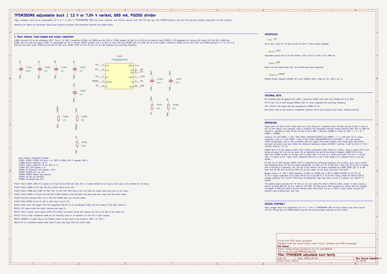
Block orb_weaver_tpsm365r6_adjustable:tpsm365r6_adjustable_12v placed in /brake_torque_sensor of mouse-joystick-pcb. High-voltage input to an adjustable 12 V or 7 V rail: TI TPSM365R6F 600 mA buck module, one family source with the FB top leg, the PGOOD bottom leg and the second output capacitor as the variant.
| Lifecycle | routed |
| Family | tpsm365r6_adjustable 12v (buck): 12 V (FB 110 k over 10 k; PGOOD 10 k over 4.7 k, 3.84 V high; two 10 uF output capacitors) |
| Placement | anchor (35, -29) mm, rotation 180°, front side; anchor rule: inferred (block not in the anchor table): the footprint with most pads |
| Sheet | hv_to_12v_tpsm365r6.kicad_sch; sheet pins: the library's arrangement |
| Drawing | mouse-joystick-pcb-brake_torque_sensor-hv_to_12v_tpsm365r6.svg |
On the Board
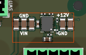
Block 4 of the board view: 19.8 × 9.7 mm on the top side, its centre 33.8 mm right of and 27.9 mm above the board centre (X right, Y up, as the enclosure tables); 13 footprints. The picture is the top render clipped around the block, the rectangle the extent of its footprints' courtyards.
Description
High-voltage input to a regulated 12 V (FB 110 k over 10 k; PGOOD 10 k over 4.7 k, 3.84 V high; two 10 uF output capacitors) step-down supply: TI TPSM365R6FRDNR adjustable (1 to 13 V) 600 mA buck module, FB divider 110k over 10k against the 1.000 V reference, PGOOD divider 10k over 4.7k from VOUT, RT 7.87k. Ports VIN, VOUT, PGOOD, GND. Output voltage, PGOOD level and capacitor ratings judged from the datasheet facts at publication (release.json); hardware validation pending. BUCK profile. VIN 3.6 V to 65 V (facts, recommended operating); the block's input capacitors are 100 V 1206 parts and its VIN copper is block-local (PWR_HV_LOCAL), so the board's power entry carries its own class. 600 mA output; the module integrates the inductor; VCC bypass and the 100 nF high-frequency input bypass are the block's. PGOOD is the module's open-drain window-comparator output (rising at about 107 %, falling at about 94 % of the set point); the block pulls it up as its description says. Adjustable variant: pin 9 is FB (divider against the 1.000 V reference, VOUT = 1 V x (1 + Rtop/Rbottom)) and pin 11 is RT (7.87 k sets the switching frequency; a block value, not a variant). The PGOOD port is the divider midpoint: 3.84 V high on the 12 V variant, above a 3.3 V logic input's absolute maximum, so a 3.3 V host needs a 5 V-tolerant input or its own divider; 3.52 V on the 7 V variant
Ports
The brief's shape, edge, class and meaning for each port, then what the board wires it to.
| Port | Shape | Edge | Class | Wired to | Board net | Board class | GPIO | Meaning | On this board |
|---|---|---|---|---|---|---|---|---|---|
GND |
passive | west | PWR_RETURN_LOCAL | GND |
/GND |
PWR_RETURN_LOCAL | Return for the module (pin 10), the dividers and every capacitor. | ||
PGOOD |
output | west | Default | PG_12V |
/PG_12V |
Default | PGOOD divider midpoint (R18002 10 k over R18003): 3.84 V high on 12v, 3.52 V on 7v. | ||
VIN |
passive | west | PWR_HV_LOCAL | +36V |
/+36V_SW |
PWR_HV_BUS | 3.6 to 65 V input on VIN (pin 3) and EN (pin 2, tied: always enabled). | ||
VOUT |
passive | west | PWR_12V_LOCAL | +12V |
/brake_torque_sensor/+12V |
PWR_12V_LOCAL | Adjustable output set by the FB divider: 12.0 V (12v) or 7.04 V (7v); 600 mA. |
Parts
As placed on the board's sheet; 13 of 13 paired with the brief's references by symbol identity, the rest given the brief's role where the internal part has one, else the catalog's role slug; the placement is the Placement field of the board's symbol, else of the library's (D38); the manufacturer part and the LCSC number are the board's BOM's.
| Reference | Brief | Part | Value | Role | Placement | Manufacturer part | LCSC | DNP |
|---|---|---|---|---|---|---|---|---|
C1901 |
C18001 |
OW-PASS-1206B105K101NT |
1uF | VIN bulk, 1 uF 100 V | beside U1901.3 (VIN), on VIN | 1206B105K101NT | C91151 | |
C1902 |
C18002 |
OW-PASS-1206B105K101NT |
1uF | VIN bulk, 1 uF 100 V | beside U1901.3 (VIN), on VIN | 1206B105K101NT | C91151 | |
C1903 |
C18003 |
OW-PASS-1206B105K101NT |
1uF | VIN bulk, 1 uF 100 V | beside U1901.3 (VIN), on VIN | 1206B105K101NT | C91151 | |
C1904 |
C18004 |
OW-PASS-GRM188R72A104KA35D |
100nF | VIN HF bypass, 100 nF | beside U1901.3 (VIN), on VIN | GRM188R72A104KA35D | C77058 | |
C1905 |
C18005 |
OW-PASS-0805B105K250NT |
1uF | VCC LDO bypass, 1 uF | beside U1901.8 (VCC), on VCC | 0805B105K250NT | C89190 | |
C1906 |
C18006 |
OW-PASS-CL31A106KAHNNNE |
10uF | Output capacitor, 10 uF | beside U1901.4 (VOUT), on VOUT | CL31A106KAHNNNE | C9807 | |
C1907 |
C18007 |
OW-PASS-CL31A106KAHNNNE |
10uF | Output capacitor, 10 uF; DNP on 7v | beside U1901.4 (VOUT), on VOUT | CL31A106KAHNNNE | C9807 | |
R1901 |
R18001 |
OW-PASS-FRC0402F7871TS |
7.87k | RT frequency-set resistor, 7.87 k | beside U1901.11 (RT), on RT | FRC0402F7871TS | C2998145 | |
R1902 |
R18002 |
OW-PASS-ERA2AEB103X |
10k | PGOOD pull-up, 10 k | beside U1901.1 (PGOOD), on PGOOD | ERA2AEB103X | C191915 | |
R1903 |
R18003 |
OW-RES-4K7-0402 |
4.7k | PGOOD bottom leg (variant) | beside U1901.1 (PGOOD), on PGOOD | 0402WGF4701TCE | C25900 | |
R1904 |
R18004 |
OW-PASS-FRC0402F1103TS |
110k | FB top leg (variant) | beside U1901.9 (FB), on FB | FRC0402F1103TS | C2909311 | |
R1905 |
R18005 |
OW-PASS-ERA2AEB103X |
10k | FB bottom leg, 10 k | beside U1901.9 (FB), on FB | ERA2AEB103X | C191915 | |
U1901 |
U18001 |
OW-PWR-TPSM365R6FRDNR |
TPSM365R6FRDNR | Buck module, integrated inductor | TPSM365R6FRDNR | C6723000 |
Operating Notes
- Signal path: VIN (3.6 to 65 V after start-up, UVLO rising 3.4 V typical) enters VIN (pin 3) and EN (pin 2, tied to VIN, so the module runs whenever input is present); the integrated-inductor module delivers VOUT (pin 4), 600 mA maximum, regulated so that FB (pin 9) sits at the 1.000 V reference (0.985 to 1.010 V): VOUT = 1 V x (1 + R18004 / R18005).
- Variants: 12v fits R18004 = 110 k (OW-PASS-FRC0402F1103TS) and R18003 = 4.7 k with both 10 uF output capacitors, 12.0 V; 7v fits R18004 = 60.4 k (OW-PASS-0402WGF6042TCE) and R18003 = 10 k and leaves C18007 unpopulated, 7.04 V. One schematic and one copper serve both variants; only those three parts differ, and each set point must stay inside the reference-tolerance window (12.000 V nominal, 11.82 to 12.12 V; 7.04 V nominal, 6.93 to 7.11 V).
- PGOOD (pin 1) is the module's open-drain window comparator (high inside the window, rising at about 107 % and falling at about 94 % of the set point, 25 us deglitch); the port is the divider midpoint, R18002 (10 k) from VOUT over R18003 to GND, so its high level is about 3.84 V on the 12 V variant and 3.52 V on the 7 V variant. 3.84 V is above a 3.3 V logic input's absolute maximum: a 3.3 V host needs a 5 V-tolerant input or its own divider.
- RT (pin 11) to GND through R18001 (7.87 k) programs the switching frequency; it is a block value, not a variant (the datasheet gives the two pin-strap frequencies, 2.2 MHz with RT at GND and 1 MHz with RT at VCC; a resistor sets a frequency in between). VCC (pin 8) is the internal LDO output, bypassed by C18005. BOOT (pin 7) is left open and the SW pins (5, 6) are tied only to each other, as the block was drawn and built.
- Bypass: three 1 uF 100 V 1206 capacitors (C18001 to C18003) and a 100 nF 0603 (C18004) at VIN; the 10 uF 25 V output capacitors sit at about 48 % (12 V) and 28 % (7 V) of their rating, inside the family's 60 % voltage-derating rule. Current limits from the datasheet: high-side short-circuit 1 A typical, low-side 0.7 A typical.
- The placing board provides the VIN entry on its own class (the block's PWR_HV_LOCAL copper is block-local), a load of at most 600 mA, its own name for the VOUT net (the port is VOUT because the variant sets the voltage; its copper is PWR_12V_LOCAL) and the thermal path: RthJA 56.3 C/W on a JEDEC 4-layer board, so give the module's pad a ground pour and vias.
Placement and Routing
Buck module, input bypass and output capacitors
C18004, C18001, C18002, C18003, U18001, C18006, C18007, C18005, R18001, R18003, R18005, R18002, R18004
U18001 converts VIN to the adjustable VOUT. Three 1 uF 100 V capacitors (C18001 to C18003) and the 100 nF C18004 bypass VIN (pin 3) to GND at the module input; C18005 (1 uF) bypasses the internal LDO output VCC (pin 8); C18006 and C18007 (10 uF) hold the output. C18007 is unpopulated on the 7v variant. R18004 (variant: 110 k or 60.4 k) from VOUT and R18005 (10 k) to GND set FB to the 1.000 V reference. R18002 (10 k) from VOUT and R18003 (variant: 4.7 k or 10 k) to GND pull the open-drain PGOOD up and set its high level. R18001 (7.87 k) from RT (pin 11) to GND programs the switching frequency.
- Place: Place C18004 (100 nF) closest to VIN (pin 3) and GND (pin 10), the 1 uF parts beside it; the input current loop is the noisiest on the block.
- Place: Place C18005 at VCC (pin 8) with a short return to pin 10.
- Place: Place C18006 and C18007 at VOUT (pin 4) with their GND ends at pin 10; keep the output loop short and on one layer.
- Place: Place R18005 at FB (pin 9) and GND, R18004 beside it; the FB node must stay short and away from the switch node.
- Place: Anywhere between VOUT, pin 1 and the PGOOD port; low-current nodes.
- Place: Place R18001 at pin 11 with a short return to pin 10.
- Route: Wide, short VIN copper from the capacitors into pin 3; no via between C18004 and the module if the layer allows it.
- Route: VCC stays inside the block; nothing else loads it.
- Route: VOUT is block-local copper (PWR_12V_LOCAL); the board names and classes the net on its side of the sheet pin.
- Route: FB is a high-impedance node: no via stitching under it, no parallel run with VIN or VOUT copper.
- Route: PGOOD is a logic flag on the Default class; its high level is the divider's, 3.84 V or 3.52 V.
- Route: RT is a sensitive analog node; keep it short and away from the switch node.
Library Identity
| Block | orb_weaver_tpsm365r6_adjustable:tpsm365r6_adjustable_12v |
| Resolution | the placed id is in the library |
| Brief | design_block_families/tpsm365r6_adjustable/source/tpsm365r6_adjustable.brief.yaml, the family's brief |
| Published sheet | 2bee772afd47a7db |
| Published PCB | 0be84ed5ca6597c3 |
| Family release | tpsm365r6_adjustable variant 12v, profile buck; 12 V (FB 110 k over 10 k; PGOOD 10 k over 4.7 k, 3.84 V high; two 10 uF output capacitors); geometry 097e1aeb511a23b1; copper 72e9bbd61c5b742f; hardware unvalidated; qualification matches |
| Placed sheet | 946784efff88a092: matches the brief: its 13 parts by internal part, every port by name and shape; the file is the board's copy under its own designators |
| Netlist check | ok on 2026-10-15: every pin on the brief's net; 14 identity records differ, the board's own instances |