hv_input_36V_terminal_2pos_5p08_protected_vertical
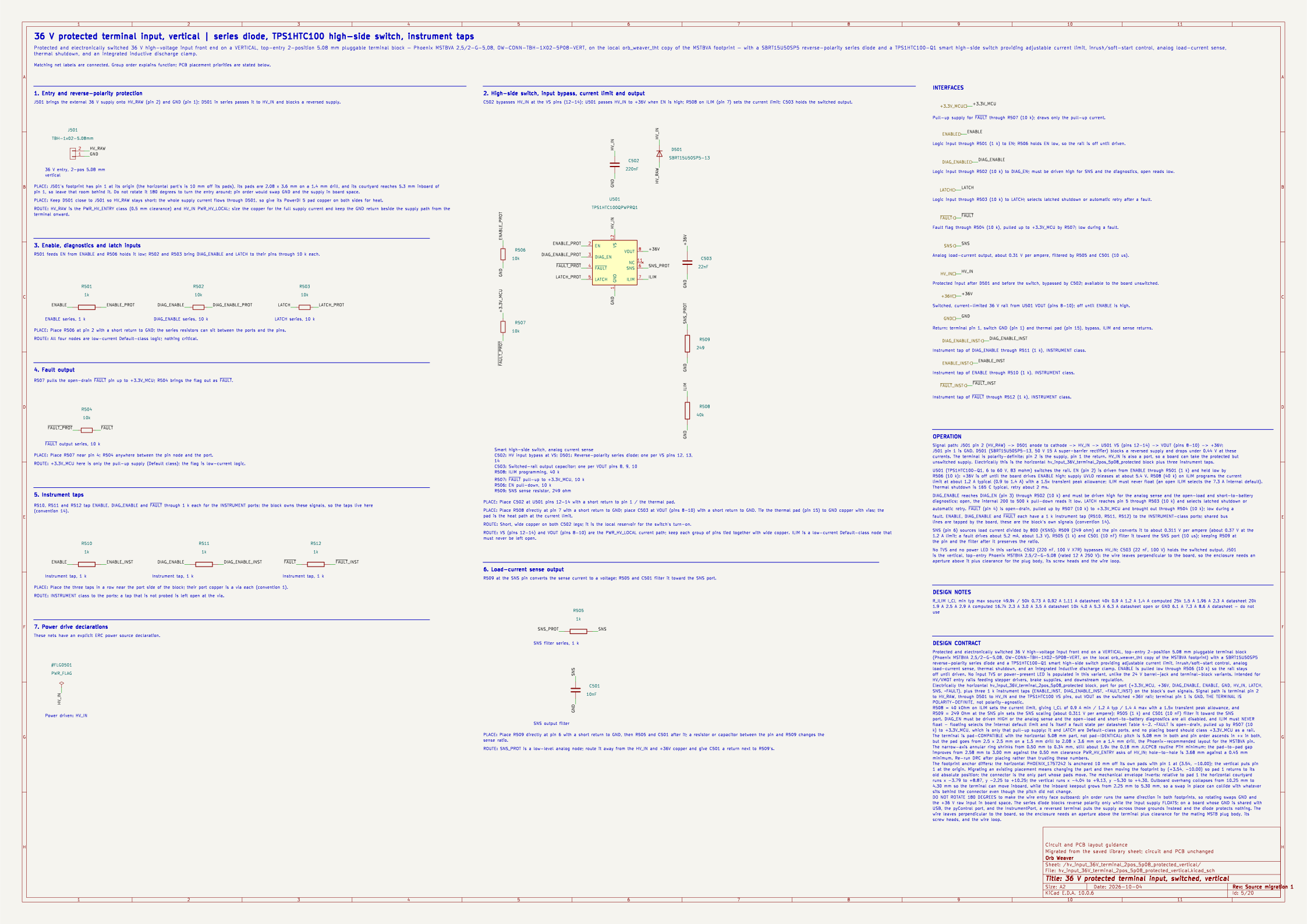
Block orb_weaver_private:hv_input_36V_terminal_2pos_5p08_protected_vertical placed in / of mouse-joystick-pcb. Protected and electronically switched 36 V high-voltage input front end on a VERTICAL, top-entry 2-position 5.08 mm pluggable terminal block — Phoenix MSTBVA 2,5/2-G-5,08, OW-CONN-TBH-1X02-5P08-VERT, on the local orb_weaver_tht copy of the MSTBVA footprint — with a SBRT15U50SP5 reverse-polarity series diode and a TPS1HTC100-Q1 smart high-side switch providing adjustable current limit, inrush/soft-start control, analog load-current sense, thermal shutdown, and an integrated inductive discharge clamp.
| Lifecycle | routed |
| Family | none (a private block) |
| Placement | anchor (-44, -24) mm, rotation 270°, front side |
| Sheet | hv_input_36V_terminal_2pos_5p08_protected_vertical.kicad_sch; sheet pins: the board's own arrangement |
| Drawing | mouse-joystick-pcb-hv_input_36V_terminal_2pos_5p08_protected_vertical.svg |
On the Board
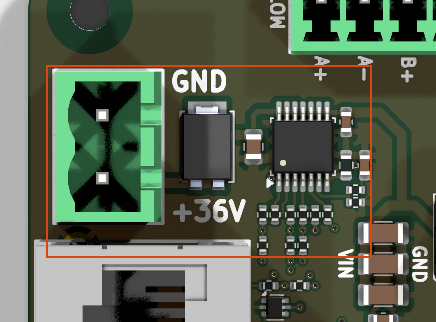
Block 1 of the board view: 26.3 × 15.5 mm on the top side, its centre 35.2 mm left of and 22.8 mm above the board centre (X right, Y up, as the enclosure tables); 18 footprints. The picture is the top render clipped around the block, the rectangle the extent of its footprints' courtyards.
Description
Protected and electronically switched 36 V high-voltage input front end on a VERTICAL, top-entry 2-position 5.08 mm pluggable terminal block (Phoenix MSTBVA 2,5/2-G-5,08, OW-CONN-TBH-1X02-5P08-VERT, on the local orb_weaver_tht copy of the MSTBVA footprint) with a SBRT15U50SP5 reverse-polarity series diode and a TPS1HTC100-Q1 smart high-side switch providing adjustable current limit, inrush/soft-start control, analog load-current sense, thermal shutdown, and an integrated inductive discharge clamp. ENABLE is pulled low through R34006 (10 k) so the rail stays off until driven. No input TVS or power-present LED is populated in this variant, unlike the 24 V barrel-jack and terminal-block variants. Intended for HV/VMOT entry rails feeding stepper drivers, brake supplies, and downstream regulation. Electrically the horizontal hv_input_36V_terminal_2pos_5p08_protected block, port for port (+3.3V_MCU, +36V, DIAG_ENABLE, ENABLE, GND, HV_IN, LATCH, SNS, ~FAULT), plus three 1 k instrument taps (ENABLE_INST, DIAG_ENABLE_INST, ~FAULT_INST) on the block's own signals. Signal path is terminal pin 2 to HV_RAW, through D34001 to HV_IN and the TPS1HTC100 VS pins, out VOUT as the switched +36V rail; terminal pin 1 is GND. THE TERMINAL IS POLARITY-DEFINITE, not polarity-agnostic. R34008 = 40 kOhm on ILIM sets the current limit, giving I_CL of 0.9 A min / 1.2 A typ / 1.4 A max with a 1.5x transient peak allowance, and R34009 = 249 Ohm at the SNS pin sets the SNS scaling (about 0.311 V per ampere); R34005 (1 k) and C34001 (10 nF) filter it toward the SNS port. DIAG_EN must be driven HIGH or the analog sense and the open-load and short-to-battery diagnostics are all disabled, and ILIM must NEVER float - floating selects the internal default limit and is itself a fault state per datasheet Table 4-2. ~FAULT is open-drain, pulled up by R34007 (10 k) to +3.3V_MCU, which is only that pull-up supply: it and LATCH are Default-class ports, and no placing board should class +3.3V_MCU as a rail. The terminal is pad-COMPATIBLE with the horizontal 5.08 mm part, not pad-IDENTICAL: pitch is 5.08 mm in both and pin order ascends in +x in both, but the pad goes from 2.5 x 2.5 mm on a 1.5 mm drill to 2.08 x 3.6 mm on a 1.4 mm drill, the Phoenix-recommended layout for the MSTBVA pin. The narrow-axis annular ring shrinks from 0.50 mm to 0.34 mm, still about 1.9x the 0.18 mm JLCPCB routine PTH minimum; the pad-to-pad gap improves from 2.58 mm to 3.00 mm against the 0.50 mm clearance PWR_HV_ENTRY asks of HV_IN; hole-to-hole is 3.68 mm against a 0.45 mm minimum. Re-run DRC after placing rather than trusting these numbers. The footprint anchor differs: the horizontal PHOENIX_1757242 is anchored 10 mm off its own pads with pin 1 at (3.54, -10.00); the vertical puts pin 1 at the origin. Migrating an existing placement means changing the part and then moving the footprint by (+3.54, -10.00) so pad 1 returns to its old absolute position; the connector is the only part whose pads move. The mechanical envelope inverts: relative to pad 1 the horizontal courtyard runs x -3.79 to +8.87, y -2.25 to +10.25; the vertical runs x -4.04 to +9.13, y -5.30 to +4.30. Outboard overhang collapses from 10.25 mm to 4.30 mm so the terminal can move inboard, while the inboard keepout grows from 2.25 mm to 5.30 mm, so a swap in place can collide with whatever sits behind the connector even though the pitch did not change. DO NOT ROTATE 180 DEGREES to make the wire entry face outboard: pin order runs the same direction in both footprints, so rotating swaps GND and the +36 V raw input in board space. The series diode blocks reverse polarity only while the input supply FLOATS; on a board whose GND is shared with USB, the pyControl port, and the InstrumentPort, a reversed terminal puts the supply across those grounds instead and the diode protects nothing. The wire leaves perpendicular to the board, so the enclosure needs an aperture above the terminal plus clearance for the mating MSTB plug body, its screw heads, and the wire loop.
Ports
The brief's shape, edge, class and meaning for each port, then what the board wires it to.
| Port | Shape | Edge | Class | Wired to | Board net | Board class | GPIO | Meaning | On this board |
|---|---|---|---|---|---|---|---|---|---|
+3.3V_MCU |
passive | west | Default | +3.3V_MCU |
/+3.3V_MCU |
PWR_3V3 | Pull-up supply for ~{FAULT} through R34007 (10 k); draws only the pull-up current. | ||
+36V |
passive | east | PWR_HV_LOCAL | +36V_SW |
/+36V_SW |
PWR_HV_BUS | Switched, current-limited 36 V rail from U34001 VOUT (pins 8-10); off until ENABLE is high. | ||
DIAG_ENABLE |
input | west | Default | HV_DIAG_EN |
/HV_DIAG_EN |
MCU_FINE | GP14 |
Logic input through R34002 (10 k) to DIAG_EN; must be driven high for SNS and the diagnostics, open reads low. | 36 V switch diagnostics enable⁵; out as the MCU sees it |
DIAG_ENABLE_INST |
output | east | INSTRUMENT | HV_DIAG_EN_INST |
/HV_DIAG_EN_INST |
INSTRUMENT | Instrument tap of DIAG_ENABLE through R34011 (1 k), INSTRUMENT class. | ||
ENABLE |
input | west | Default | HV_EN |
/HV_EN |
MCU_FINE | GP19 |
Logic input through R34001 (1 k) to EN; R34006 holds EN low, so the rail is off until driven. | 36 V input switch enable; out as the MCU sees it |
ENABLE_INST |
output | east | INSTRUMENT | HV_EN_INST |
/HV_EN_INST |
INSTRUMENT | Instrument tap of ENABLE through R34010 (1 k), INSTRUMENT class. | ||
GND |
passive | east | PWR_RETURN_LOCAL | GND |
/GND |
PWR_RETURN_LOCAL | Return: terminal pin 1, switch GND (pin 1) and thermal pad (pin 15), bypass, ILIM and sense returns. | ||
HV_IN |
passive | east | PWR_HV_LOCAL | open: no-connect flag | Protected input after D34001 and before the switch, bypassed by C34002; available to the board unswitched. | ||||
LATCH |
input | west | Default | HV_LATCH |
/HV_LATCH |
MCU_FINE | GP24 |
Logic input through R34003 (10 k) to LATCH; selects latched shutdown or automatic retry after a fault. | 36 V switch latch-off select¹⁰; out as the MCU sees it |
SNS |
output | west | Default | HV_SNS |
/HV_SNS |
MCU_FINE | GP28 |
Analog load-current output, about 0.31 V per ampere, filtered by R34005 and C34001 (10 us). | 36 V input load-current sense, R_SNS = 249 Ω; in as the MCU sees it |
~{FAULT} |
output | west | Default | ~{HV_FAULT} |
/~{HV_FAULT} |
MCU_FINE | GP23 |
Fault flag through R34004 (10 k), pulled up to +3.3V_MCU by R34007; low during a fault. | 36 V switch fault, open-drain, pull-up 3.3 V¹¹; in as the MCU sees it |
~{FAULT}_INST |
output | east | INSTRUMENT | ~{HV_FAULT}_INST |
/~{HV_FAULT}_INST |
INSTRUMENT | Instrument tap of ~{FAULT} through R34012 (1 k), INSTRUMENT class. |
Parts
As placed on the board's sheet; 18 of 18 paired with the brief's references by symbol identity, the rest given the brief's role where the internal part has one, else the catalog's role slug; the placement is the Placement field of the board's symbol, else of the library's (D38); the manufacturer part and the LCSC number are the board's BOM's.
| Reference | Brief | Part | Value | Role | Placement | Manufacturer part | LCSC | DNP |
|---|---|---|---|---|---|---|---|---|
C501 |
C34001 |
OW-CAP-10N-0603-X7R-50V |
10nF | SNS output filter | CC0603JRX7R9BB103 | C115056 | ||
C502 |
C34002 |
OW-CAP-220N-0805-X7R-100V |
220nF | HV input bypass at VS | beside U501 VS pins 12, 13, 14 (one per pin), on HV_IN | CC0805KKX7R0BB224 | C513710 | |
C503 |
C34003 |
OW-PASS-GCM188R72A223KA37D |
22nF | Switched-rail output capacitor | beside U501 VOUT pins 8, 9, 10 (one per pin), on +36V | GCM188R72A223KA37D | C161234 | |
D501 |
D34001 |
OW-MISC-SBRT15U50SP5-13 |
SBRT15U50SP5-13 | Reverse-polarity series diode | beside U501 VS pins 12, 13, 14 (one per pin), on HV_IN | SBRT15U50SP5-13 | C211388 | |
J501 |
J34001 |
OW-CONN-TBH-1X02-5P08-VERT |
TBH-1x02-5.08mm | 36 V entry, 2-pos 5.08 mm vertical | 1755736 | C480503 | ||
R501 |
R34001 |
OW-PASS-RC0402FR-071KL |
1k | ENABLE series, 1 k | RC0402FR-071KL | C106235 | ||
R502 |
R34002 |
OW-RES-10K-0402 |
10k | DIAG_ENABLE series, 10 k | ERJ2GEJ103X | C278577 | ||
R503 |
R34003 |
OW-RES-10K-0402 |
10k | LATCH series, 10 k | ERJ2GEJ103X | C278577 | ||
R504 |
R34004 |
OW-RES-10K-0402 |
10k | ~{FAULT} output series, 10 k | ERJ2GEJ103X | C278577 | ||
R505 |
R34005 |
OW-PASS-RC0402FR-071KL |
1k | SNS filter series, 1 k | RC0402FR-071KL | C106235 | ||
R506 |
R34006 |
OW-RES-10K-0402 |
10k | EN pull-down, 10 k | beside U501.2 (EN), on ENABLE_PROT | ERJ2GEJ103X | C278577 | |
R507 |
R34007 |
OW-RES-10K-0402 |
10k | ~{FAULT} pull-up to +3.3V_MCU, 10 k | beside U501.4 (~{FAULT}), on ~{FAULT_PROT} | ERJ2GEJ103X | C278577 | |
R508 |
R34008 |
OW-PASS-SCR0603F40K |
40k | ILIM programming, 40 k | beside U501.7 (ILIM), on ILIM | SCR0603F40K | C3016445 | |
R509 |
R34009 |
OW-PASS-CRCW0402249RFKED |
249 | SNS sense resistor, 249 ohm | beside U501.6 (SNS), on SNS_PROT | CRCW0402249RFKED | C482112 | |
R510 |
R34010 |
OW-PASS-RC0402FR-071KL |
1k | Instrument tap, 1 k | RC0402FR-071KL | C106235 | ||
R511 |
R34011 |
OW-PASS-RC0402FR-071KL |
1k | Instrument tap, 1 k | RC0402FR-071KL | C106235 | ||
R512 |
R34012 |
OW-PASS-RC0402FR-071KL |
1k | Instrument tap, 1 k | RC0402FR-071KL | C106235 | ||
U501 |
U34001 |
OW-PWR-TPS1HTC100QPWPRQ1 |
TPS1HTC100QPWPRQ1 | Smart high-side switch, analog current sense | TPS1HTC100QPWPRQ1 | C41558366 |
Operating Notes
- Signal path: J34001 pin 2 (HV_RAW) -> D34001 anode to cathode -> HV_IN -> U34001 VS (pins 12-14) -> VOUT (pins 8-10) -> +36V; J34001 pin 1 is GND. D34001 (SBRT15U50SP5-13, 50 V 15 A super-barrier rectifier) blocks a reversed supply and drops under 0.44 V at these currents. The terminal is polarity-definite: pin 2 is the supply, pin 1 the return. HV_IN is also a port, so a board can take the protected but unswitched supply. Electrically this is the horizontal hv_input_36V_terminal_2pos_5p08_protected block plus three instrument taps.
- U34001 (TPS1HTC100-Q1, 6 to 60 V, 83 mohm) switches the rail. EN (pin 2) is driven from ENABLE through R34001 (1 k) and held low by R34006 (10 k): +36V is off until the board drives ENABLE high; supply UVLO releases at about 5.4 V. R34008 (40 k) on ILIM programs the current limit at about 1.2 A typical (0.9 to 1.4 A) with a 1.5x transient peak allowance; ILIM must never float (an open ILIM selects the 7.3 A internal default). Thermal shutdown is 165 C typical, retry about 2 ms.
- DIAG_ENABLE reaches DIAG_EN (pin 3) through R34002 (10 k) and must be driven high for the analog sense and the open-load and short-to-battery diagnostics; open, the internal 200 to 500 k pull-down reads it low. LATCH reaches pin 5 through R34003 (10 k) and selects latched shutdown or automatic retry. ~{FAULT} (pin 4) is open-drain, pulled up by R34007 (10 k) to +3.3V_MCU and brought out through R34004 (10 k); low during a fault. ENABLE, DIAG_ENABLE and ~{FAULT} each have a 1 k instrument tap (R34010, R34011, R34012) to the INSTRUMENT-class ports; shared bus lines are tapped by the board, these are the block's own signals (convention 14).
- SNS (pin 6) sources load current divided by 800 (KSNS): R34009 (249 ohm) at the pin converts it to about 0.311 V per ampere (about 0.37 V at the 1.2 A limit; a fault drives about 5.2 mA, about 1.3 V). R34005 (1 k) and C34001 (10 nF) filter it toward the SNS port (10 us); keeping R34009 at the pin and the filter after it preserves the ratio.
- No TVS and no power LED in this variant. C34002 (220 nF, 100 V X7R) bypasses HV_IN; C34003 (22 nF, 100 V) holds the switched output. J34001 is the vertical, top-entry Phoenix MSTBVA 2,5/2-G-5,08 (rated 12 A 250 V): the wire leaves perpendicular to the board, so the enclosure needs an aperture above it plus clearance for the plug body, its screw heads and the wire loop.
Placement and Routing
Entry and reverse-polarity protection
J34001
J34001 brings the external 36 V supply onto HV_RAW (pin 2) and GND (pin 1); D34001 in series passes it to HV_IN and blocks a reversed supply.
- Place: J34001's footprint has pin 1 at its origin (the horizontal part's is 10 mm off its pads), its pads are 2.08 x 3.6 mm on a 1.4 mm drill, and its courtyard reaches 5.3 mm inboard of pin 1, so leave that room behind it. Do not rotate it 180 degrees to turn the entry around; pin order would swap GND and the supply in board space.
- Place: Keep D34001 close to J34001 so HV_RAW stays short; the whole supply current flows through D34001, so give its PowerDI 5 pad copper on both sides for heat.
- Route: HV_RAW is the PWR_HV_ENTRY class (0.5 mm clearance) and HV_IN PWR_HV_LOCAL; size the copper for the full supply current and keep the GND return beside the supply path from the terminal onward.
High-side switch, input bypass, current limit and output
C34002, U34001, R34008, C34003, R34007, R34006, R34009, D34001
C34002 bypasses HV_IN at the VS pins (12-14); U34001 passes HV_IN to +36V when EN is high; R34008 on ILIM (pin 7) sets the current limit; C34003 holds the switched output.
- Place: Place C34002 at U34001 pins 12-14 with a short return to pin 1 / the thermal pad.
- Place: Place R34008 directly at pin 7 with a short return to GND; place C34003 at VOUT (pins 8-10) with a short return to GND. Tie the thermal pad (pin 15) to GND copper with vias; the pad is the heat path at the current limit.
- Route: Short, wide copper on both C34002 legs; it is the local reservoir for the switch's turn-on.
- Route: VS (pins 12-14) and VOUT (pins 8-10) are the PWR_HV_LOCAL current path; keep each group of pins tied together with wide copper. ILIM is a low-current Default-class node that must never be left open.
Enable, diagnostics and latch inputs
R34001, R34002, R34003
R34001 feeds EN from ENABLE and R34006 holds it low; R34002 and R34003 bring DIAG_ENABLE and LATCH to their pins through 10 k each.
- Place: Place R34006 at pin 2 with a short return to GND; the series resistors can sit between the ports and the pins.
- Route: All four nodes are low-current Default-class logic; nothing critical.
Fault output
R34004
R34007 pulls the open-drain ~{FAULT} pin up to +3.3V_MCU; R34004 brings the flag out as ~{FAULT}.
- Place: Place R34007 near pin 4; R34004 anywhere between the pin node and the port.
- Route: +3.3V_MCU here is only the pull-up supply (Default class); the flag is low-current logic.
Instrument taps
R34010, R34011, R34012
R34010, R34011 and R34012 tap ENABLE, DIAG_ENABLE and ~{FAULT} through 1 k each for the INSTRUMENT ports; the block owns these signals, so the taps live here (convention 14).
- Place: Place the three taps in a row near the port side of the block; their port copper is a via each (convention 1).
- Route: INSTRUMENT class to the ports; a tap that is not probed is left open at the via.
Load-current sense output
R34005, C34001
R34009 at the SNS pin converts the sense current to a voltage; R34005 and C34001 filter it toward the SNS port.
- Place: Place R34009 directly at pin 6 with a short return to GND, then R34005 and C34001 after it; a resistor or capacitor between the pin and R34009 changes the sense ratio.
- Route: SNS_PROT is a low-level analog node; route it away from the HV_IN and +36V copper and give C34001 a return next to R34009's.
Library Identity
| Block | orb_weaver_private:hv_input_36V_terminal_2pos_5p08_protected_vertical |
| Resolution | the placed id is in the library |
| Brief | design_blocks/orb_weaver_private.kicad_blocks/hv_input_36V_terminal_2pos_5p08_protected_vertical.kicad_block/hv_input_36V_terminal_2pos_5p08_protected_vertical.brief.yaml, the block's brief |
| Published sheet | a3d735d1cbae1ba8 |
| Published PCB | 868d8e9a3b3dcb73 |
| Source lock | symbol snapshot 126daeb69a2d9a76, published 2026-10-14 |
| Placed sheet | 0aa5c86bce0f5cf9: matches the brief: its 18 parts by internal part, every port by name and shape; the file is the board's copy under its own designators |
| Netlist check | ok on 2026-10-15: every pin on the brief's net; 21 identity records differ, the board's own instances |