5v_to_3v3_tps73733_2
Block orb_weaver_private:5v_to_3v3_tps73733 placed in / of mouse-joystick-pcb. Clean 3.3 V linear regulator from a 5 V input rail using the TI TPS73733 fixed 3.3 V 1 A LDO.
| Lifecycle | routed |
| Family | none (a private block) |
| Placement | anchor (-14, 1.75) mm, rotation 180°, front side; as built: -14, 1.75 is off the 1 mm grid (review) |
| Sheet | 5v_to_3v3_tps73733_2.kicad_sch; sheet pins: the board's own arrangement |
| Drawing | mouse-joystick-pcb-5v_to_3v3_tps73733_2.svg |
On the Board
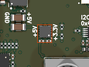
Block 12 of the board view: 3.9 × 4.9 mm on the top side, its centre 14.0 mm left of and 2.3 mm below the board centre (X right, Y up, as the enclosure tables); 3 footprints. The picture is the top render clipped around the block, the rectangle the extent of its footprints' courtyards.
Description
Clean 3.3 V linear regulator from a 5 V input rail using the TI TPS73733 fixed 3.3 V 1 A LDO. Intended for MCU, RP2040, TMC logic, encoder interface, and other low-voltage digital circuitry.
Ports
The brief's shape, edge, class and meaning for each port, then what the board wires it to.
| Port | Shape | Edge | Class | Wired to | Board net | Board class | GPIO | Meaning | On this board |
|---|---|---|---|---|---|---|---|---|---|
+3.3V |
passive | east | PWR_3V3_LOCAL | +3.3V_SW |
/+3.3V_SW |
PWR_3V3 | Regulated output, 3.3 V fixed. | ||
+5V |
passive | west | PWR_5V_LOCAL | +5V_SW |
/+5V_SW |
PWR_5V | Input rail; also drives EN, so the regulator is on whenever it is present. | ||
GND |
passive | west | PWR_RETURN_LOCAL | GND |
/GND |
PWR_RETURN_LOCAL | Common return; regulator ground pin and thermal pad. |
Parts
As placed on the board's sheet; 3 of 3 paired with the brief's references by symbol identity, the rest given the brief's role where the internal part has one, else the catalog's role slug; the placement is the Placement field of the board's symbol, else of the library's (D38); the manufacturer part and the LCSC number are the board's BOM's.
| Reference | Brief | Part | Value | Role | Placement | Manufacturer part | LCSC | DNP |
|---|---|---|---|---|---|---|---|---|
C1001 |
C14001 |
OW-PASS-CL05A105KL5NRNC |
1uF | Input bypass | beside U1001.5 (EN), on +5V | CL05A105KL5NRNC | C307413 | |
C1002 |
C14002 |
OW-PASS-CL05A105KL5NRNC |
1uF | Output capacitor | beside U1001.1 (OUT), on +3.3V | CL05A105KL5NRNC | C307413 | |
U1001 |
U14001 |
OW-PWR-TPS73733QDRBRQ1 |
TPS73733QDRBRQ1 | Fixed 3.3 V LDO | TPS73733QDRBRQ1 | C523768 |
Operating Notes
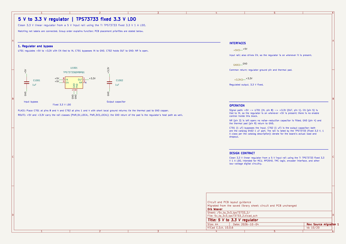
- Signal path: +5V -> U14001 (IN, pin 8) -> +3.3V (OUT, pin 1). EN (pin 5) is tied to IN, so the regulator is on whenever +5V is present; there is no enable control inside this block.
- NR (pin 3) is left open: no noise-reduction capacitor is fitted. GND (pin 4) and the thermal pad (pin 9) return to GND.
- C14001 (1 uF) bypasses the input, C14002 (1 uF) is the output capacitor; both are the catalog 0402 1 uF part. The rail is rated by the TPS73733 (fixed 3.3 V, 1 A class per the catalog description); derate for the board's actual load and dropout.
Placement and Routing
Regulator and bypass
C14001, U14001, C14002
U14001 regulates +5V to +3.3V with EN tied to IN. C14001 bypasses IN to GND, C14002 holds OUT to GND; NR is open.
- Place: Place C14001 at pins 8 and 4 and C14002 at pins 1 and 4 with short local ground returns; tie the thermal pad to GND copper.
- Route: +5V and +3.3V carry the rail classes (PWR_5V_LOCAL, PWR_3V3_LOCAL); the GND return of the pad is the regulator's heat path as well.
Library Identity
| Block | orb_weaver_private:5v_to_3v3_tps73733 |
| Resolution | the placed id is in the library |
| Brief | design_blocks/orb_weaver_private.kicad_blocks/5v_to_3v3_tps73733.kicad_block/5v_to_3v3_tps73733.brief.yaml, the block's brief |
| Published sheet | d047d03bb7b59ea0 |
| Published PCB | 7de227e948431743 |
| Source lock | symbol snapshot 1238ec2a0373421b, published 2026-10-14 |
| Placed sheet | 6e26116757766e55: matches the brief: its 3 parts by internal part, every port by name and shape; the file is the board's copy under its own designators |
| Netlist check | ok on 2026-10-15: every pin on the brief's net; 4 identity records differ, the board's own instances |