logic_input_2ch_5v_schmitt_sn74lvc2g17
Block orb_weaver_private:logic_input_2ch_5v_schmitt_sn74lvc2g17 placed in /inputs of camera-gpio-interface-pcb. Two-channel single-ended logic input conditioner: per-channel series/RC filtering plus an SN74LVC2G17 dual Schmitt-trigger buffer that turns a 3.3 V or 5 V field-wired logic signal into clean 3.3 V logic, with a 100 ohm InstrumentPort tap on each output.
| Lifecycle | routed |
| Family | none (a private block) |
| Placement | anchor (-12, 17) mm, rotation 90°, front side |
| Sheet | logic_input_2ch_5v_schmitt_sn74lvc2g17.kicad_sch; sheet pins: the board's own arrangement |
| Drawing | camera-gpio-interface-pcb-inputs-logic_input_2ch_5v_schmitt_sn74lvc2g17.svg |
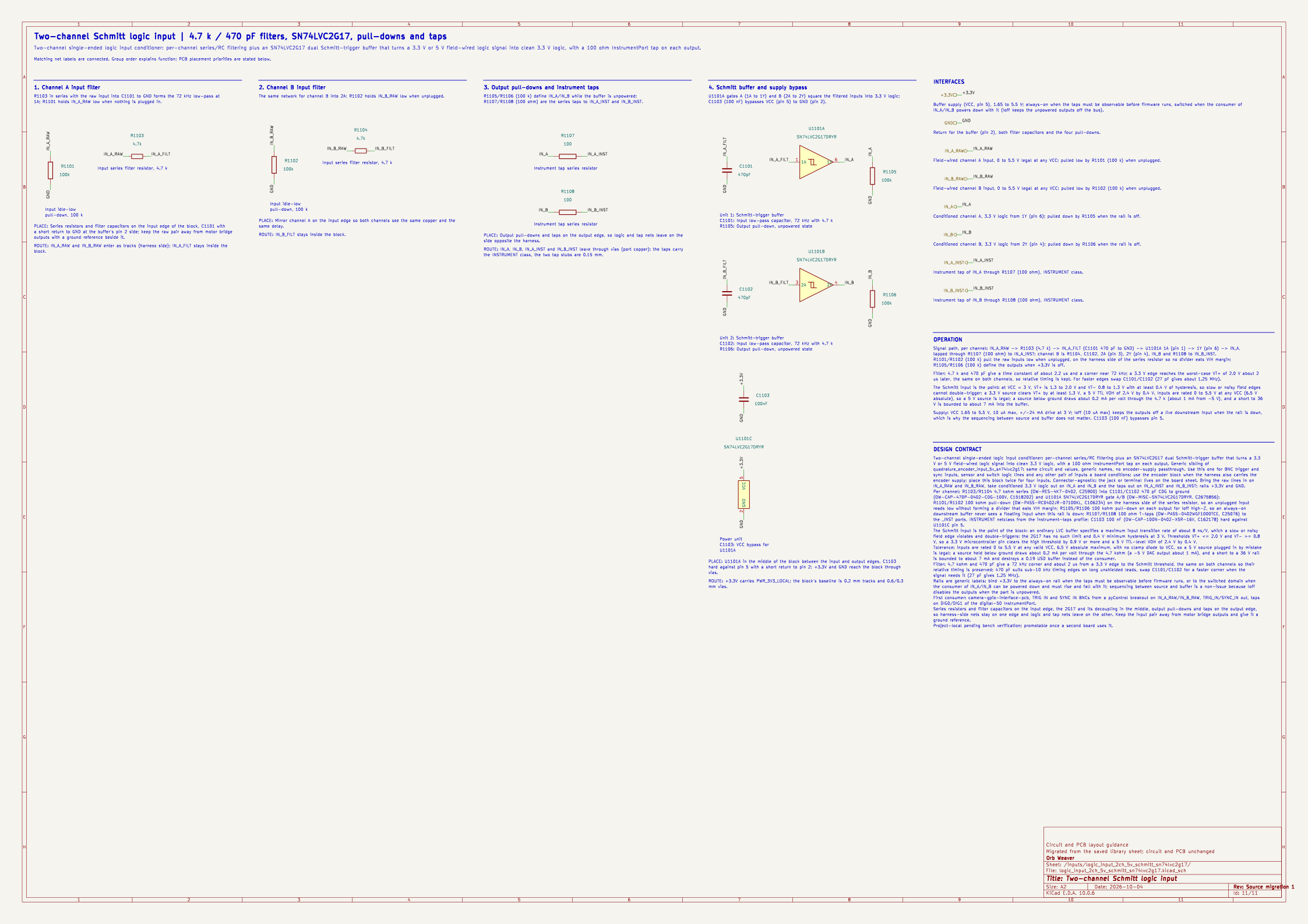
On the Board
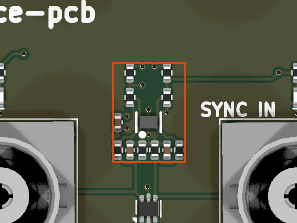
Block 7 of the board view: 5.9 × 8.1 mm on the top side, its centre 12.0 mm left of and 16.1 mm below the board centre (X right, Y up, as the enclosure tables); 12 footprints. The picture is the top render clipped around the block, the rectangle the extent of its footprints' courtyards.
Description
Two-channel single-ended logic input conditioner: per-channel series/RC filtering plus an SN74LVC2G17 dual Schmitt-trigger buffer that turns a 3.3 V or 5 V field-wired logic signal into clean 3.3 V logic, with a 100 ohm InstrumentPort tap on each output. Generic sibling of quadrature_encoder_input_5v_sn74lvc2g17: same circuit and values, generic names, no encoder-supply passthrough. Use this one for BNC trigger and sync inputs, sensor and switch logic lines and any other pair of inputs a board conditions; use the encoder block when the harness also carries the encoder supply; place this block twice for four inputs. Connector-agnostic: the jack or terminal lives on the board sheet. Bring the raw lines in on IN_A_RAW and IN_B_RAW, take conditioned 3.3 V logic out on IN_A and IN_B and the taps out on IN_A_INST and IN_B_INST; rails +3.3V and GND. Per channel: R41003/R41004 4.7 kohm series (OW-RES-4K7-0402, C25900) into C41001/C41002 470 pF C0G to ground (OW-CAP-470P-0402-C0G-100V, C1518202) and U41001 SN74LVC2G17DRYR gate A/B (OW-MISC-SN74LVC2G17DRYR, C2675856); R41001/R41002 100 kohm pull-down (OW-PASS-RC0402JR-07100KL, C106234) on the harness side of the series resistor, so an unplugged input reads low without forming a divider that eats VIH margin; R41005/R41006 100 kohm pull-down on each output for Ioff high-Z, so an always-on downstream buffer never sees a floating input when this rail is down; R41007/R41008 100 ohm T-taps (OW-PASS-0402WGF1000TCE, C25076) to the _INST ports, INSTRUMENT netclass from the instrument-taps profile; C41003 100 nF (OW-CAP-100N-0402-X5R-16V, C162178) hard against U41001 pin 5. The Schmitt input is the point of the block: an ordinary LVC buffer specifies a maximum input transition rate of about 8 ns/V, which a slow or noisy field edge violates and double-triggers; the 2G17 has no such limit and 0.4 V minimum hysteresis at 3 V. Thresholds VT+ <= 2.0 V and VT- >= 0.8 V, so a 3.3 V microcontroller pin clears the high threshold by 0.9 V or more and a 5 V TTL-level VOH of 2.4 V by 0.4 V. Tolerance: inputs are rated 0 to 5.5 V at any valid VCC, 6.5 V absolute maximum, with no clamp diode to VCC, so a 5 V source plugged in by mistake is legal; a source held below ground draws about 0.2 mA per volt through the 4.7 kohm (a -5 V DAC output about 1 mA), and a short to a 36 V rail is bounded to about 7 mA and destroys a 0.19 USD buffer instead of the consumer. Filter: 4.7 kohm and 470 pF give a 72 kHz corner and about 2 us from a 3.3 V edge to the Schmitt threshold, the same on both channels so their relative timing is preserved; 470 pF suits sub-10 kHz timing edges on long unshielded leads, swap C41001/C41002 for a faster corner when the signal needs it (27 pF gives 1.25 MHz). Rails are generic labels: bind +3.3V to the always-on rail when the taps must be observable before firmware runs, or to the switched domain when the consumer of IN_A/IN_B can be powered down and must rise and fall with it; sequencing between source and buffer is a non-issue because Ioff disables the outputs when the part is unpowered. First consumer: camera-gpio-interface-pcb, TRIG IN and SYNC IN BNCs from a pyControl breakout on IN_A_RAW/IN_B_RAW, TRIG_IN/SYNC_IN out, taps on DIG0/DIG1 of the digital-50 InstrumentPort. Series resistors and filter capacitors on the input edge, the 2G17 and its decoupling in the middle, output pull-downs and taps on the output edge, so harness-side nets stay on one edge and logic and tap nets leave on the other. Keep the input pair away from motor bridge outputs and give it a ground reference. Project-local pending bench verification; promotable once a second board uses it.
Ports
The brief's shape, edge, class and meaning for each port, then what the board wires it to.
| Port | Shape | Edge | Class | Wired to | Board net | Board class | GPIO | Meaning | On this board |
|---|---|---|---|---|---|---|---|---|---|
+3.3V |
passive | west | PWR_3V3_LOCAL | +3.3V |
/+3.3V |
PWR_3V3_NARROW | Buffer supply (VCC, pin 5), 1.65 to 5.5 V; always-on when the taps must be observable before firmware runs, switched when the consumer of IN_A/IN_B powers down with it (Ioff keeps the unpowered outputs off the bus). | The only logic rail, from the TPS73733 on the power sheet; always on while USB is present, as the InstrumentPort block requires | |
GND |
passive | west | PWR_RETURN_LOCAL | GND |
/GND |
PWR_RETURN_LOCAL | Return for the buffer (pin 2), both filter capacitors and the four pull-downs. | Board ground; every BNC shell and camera pins 5 and 6 | |
IN_A |
output | east | Default | TRIG_IN |
/TRIG_IN |
Default | Conditioned channel A, 3.3 V logic from 1Y (pin 6); pulled down by R41005 when the rail is off. | Conditioned 150 Hz frame trigger from the TRIG IN BNC, 3.3 V, to the three camera channels' Line 3 drivers | |
IN_A_INST |
output | east | INSTRUMENT | TRIG_IN_INST |
/TRIG_IN_INST |
INSTRUMENT | Instrument tap of IN_A through R41007 (100 ohm), INSTRUMENT class. | DIG0: the conditioned trigger after the Schmitt (the input block's IN_A_INST) | |
IN_A_RAW |
input | west | Default | TRIG_RAW |
/inputs/TRIG_RAW |
Default | Field-wired channel A input, 0 to 5.5 V legal at any VCC; pulled low by R41001 (100 k) when unplugged. | The TRIG IN jack to the ESD clamp and the input block's IN_A_RAW | |
IN_B |
output | east | Default | SYNC_IN |
/SYNC_IN |
Default | Conditioned channel B, 3.3 V logic from 2Y (pin 4); pulled down by R41006 when the rail is off. | Conditioned Rsync from the SYNC IN BNC, 3.3 V, to the three Line 0 drivers and the SYNC OUT driver | |
IN_B_INST |
output | east | INSTRUMENT | SYNC_IN_INST |
/SYNC_IN_INST |
INSTRUMENT | Instrument tap of IN_B through R41008 (100 ohm), INSTRUMENT class. | DIG1: the conditioned Rsync after the Schmitt (the input block's IN_B_INST) | |
IN_B_RAW |
input | west | Default | SYNC_RAW |
/inputs/SYNC_RAW |
Default | Field-wired channel B input, 0 to 5.5 V legal at any VCC; pulled low by R41002 (100 k) when unplugged. | The SYNC IN jack to the ESD clamp and the input block's IN_B_RAW |
Parts
As placed on the board's sheet; 12 of 12 paired with the brief's references by symbol identity, the rest given the brief's role where the internal part has one, else the catalog's role slug; the placement is the Placement field of the board's symbol, else of the library's (D38); the manufacturer part and the LCSC number are the board's BOM's.
| Reference | Brief | Part | Value | Role | Placement | Manufacturer part | LCSC | DNP |
|---|---|---|---|---|---|---|---|---|
C1101 |
C41001 |
OW-CAP-470P-0402-C0G-100V |
470pF | Input low-pass capacitor, 72 kHz with 4.7 k | beside U1101A.1 (1A), on IN_A_FILT | GRM1555C2A471JE01D | C1518202 | |
C1102 |
C41002 |
OW-CAP-470P-0402-C0G-100V |
470pF | Input low-pass capacitor, 72 kHz with 4.7 k | beside U1101B.3 (2A), on IN_B_FILT | GRM1555C2A471JE01D | C1518202 | |
C1103 |
C41003 |
OW-CAP-100N-0402-X5R-16V |
100nF | VCC bypass for U41001 | beside U1101C.5 (VCC), on +3.3V | GRM155R62A104KE14D | C162178 | |
R1101 |
R41001 |
OW-PASS-RC0402JR-07100KL |
100k | Input idle-low pull-down, 100 k | RC0402JR-07100KL | C106234 | ||
R1102 |
R41002 |
OW-PASS-RC0402JR-07100KL |
100k | Input idle-low pull-down, 100 k | RC0402JR-07100KL | C106234 | ||
R1103 |
R41003 |
OW-RES-4K7-0402 |
4.7k | Input series filter resistor, 4.7 k | 0402WGF4701TCE | C25900 | ||
R1104 |
R41004 |
OW-RES-4K7-0402 |
4.7k | Input series filter resistor, 4.7 k | 0402WGF4701TCE | C25900 | ||
R1105 |
R41005 |
OW-PASS-RC0402JR-07100KL |
100k | Output pull-down, unpowered state | beside U1101A.6 (1Y), on IN_A | RC0402JR-07100KL | C106234 | |
R1106 |
R41006 |
OW-PASS-RC0402JR-07100KL |
100k | Output pull-down, unpowered state | beside U1101B.4 (2Y), on IN_B | RC0402JR-07100KL | C106234 | |
R1107 |
R41007 |
OW-PASS-0402WGF1000TCE |
100 | Instrument tap series resistor | 0402WGF1000TCE | C25076 | ||
R1108 |
R41008 |
OW-PASS-0402WGF1000TCE |
100 | Instrument tap series resistor | 0402WGF1000TCE | C25076 | ||
U1101 |
U41001 |
OW-MISC-SN74LVC2G17DRYR |
SN74LVC2G17DRYR | Schmitt-trigger buffer | SN74LVC2G17DRYR | C2675856 |
Operating Notes
- Signal path, per channel: IN_A_RAW -> R41003 (4.7 k) -> IN_A_FILT (C41001 470 pF to GND) -> U41001 1A (pin 1) -> 1Y (pin 6) -> IN_A, tapped through R41007 (100 ohm) to IN_A_INST; channel B is R41004, C41002, 2A (pin 3), 2Y (pin 4), IN_B and R41008 to IN_B_INST. R41001/R41002 (100 k) pull the raw inputs low when unplugged, on the harness side of the series resistor so no divider eats VIH margin; R41005/R41006 (100 k) define the outputs when +3.3V is off.
- Filter: 4.7 k and 470 pF give a time constant of about 2.2 us and a corner near 72 kHz; a 3.3 V edge reaches the worst-case VT+ of 2.0 V about 2 us later, the same on both channels, so relative timing is kept. For faster edges swap C41001/C41002 (27 pF gives about 1.25 MHz).
- The Schmitt input is the point: at VCC = 3 V, VT+ is 1.3 to 2.0 V and VT- 0.8 to 1.3 V with at least 0.4 V of hysteresis, so slow or noisy field edges cannot double-trigger; a 3.3 V source clears VT+ by at least 1.3 V, a 5 V TTL VOH of 2.4 V by 0.4 V. Inputs are rated 0 to 5.5 V at any VCC (6.5 V absolute), so a 5 V source is legal; a source below ground draws about 0.2 mA per volt through the 4.7 k (about 1 mA from -5 V), and a short to 36 V is bounded to about 7 mA into the buffer.
- Supply: VCC 1.65 to 5.5 V, 10 uA max, +/-24 mA drive at 3 V; Ioff (10 uA max) keeps the outputs off a live downstream input when the rail is down, which is why the sequencing between source and buffer does not matter. C41003 (100 nF) bypasses pin 5.
Placement and Routing
Channel A input filter
R41001, R41003
R41003 in series with the raw input into C41001 to GND forms the 72 kHz low-pass at 1A; R41001 holds IN_A_RAW low when nothing is plugged in.
- Place: Series resistors and filter capacitors on the input edge of the block, C41001 with a short return to GND at the buffer's pin 2 side; keep the raw pair away from motor bridge outputs with a ground reference beside it.
- Route: IN_A_RAW and IN_B_RAW enter as tracks (harness side); IN_A_FILT stays inside the block.
Channel B input filter
R41002, R41004
The same network for channel B into 2A; R41002 holds IN_B_RAW low when unplugged.
- Place: Mirror channel A on the input edge so both channels see the same copper and the same delay.
- Route: IN_B_FILT stays inside the block.
Output pull-downs and instrument taps
R41007, R41008
R41005/R41006 (100 k) define IN_A/IN_B while the buffer is unpowered; R41007/R41008 (100 ohm) are the series taps to IN_A_INST and IN_B_INST.
- Place: Output pull-downs and taps on the output edge, so logic and tap nets leave on the side opposite the harness.
- Route: IN_A, IN_B, IN_A_INST and IN_B_INST leave through vias (port copper); the taps carry the INSTRUMENT class, the two tap stubs are 0.15 mm.
Schmitt buffer and supply bypass
U41001, C41003, C41001, C41002, R41005, R41006
U41001 gates A (1A to 1Y) and B (2A to 2Y) square the filtered inputs into 3.3 V logic; C41003 (100 nF) bypasses VCC (pin 5) to GND (pin 2).
- Place: U41001 in the middle of the block between the input and output edges, C41003 hard against pin 5 with a short return to pin 2; +3.3V and GND reach the block through vias.
- Route: +3.3V carries PWR_3V3_LOCAL; the block's baseline is 0.2 mm tracks and 0.6/0.3 mm vias.
Library Identity
| Block | orb_weaver_private:logic_input_2ch_5v_schmitt_sn74lvc2g17 |
| Resolution | the placed id is in the library |
| Brief | design_blocks/orb_weaver_private.kicad_blocks/logic_input_2ch_5v_schmitt_sn74lvc2g17.kicad_block/logic_input_2ch_5v_schmitt_sn74lvc2g17.brief.yaml, the block's brief |
| Published sheet | eb3efe0db8c09f06 |
| Published PCB | 75189b4603e8f8c5 |
| Source lock | symbol snapshot d0f8273d1ebeb5a2, published 2026-10-14 |
| Placed sheet | 768774d53281c846: matches the brief: its 12 parts by internal part, every port by name and shape; the file is the board's copy under its own designators |
| Netlist check | ok on 2026-10-15: every pin on the brief's net; 14 identity records differ, the board's own instances |