blackfly_s_gpio_channel_mcv6_vertical2
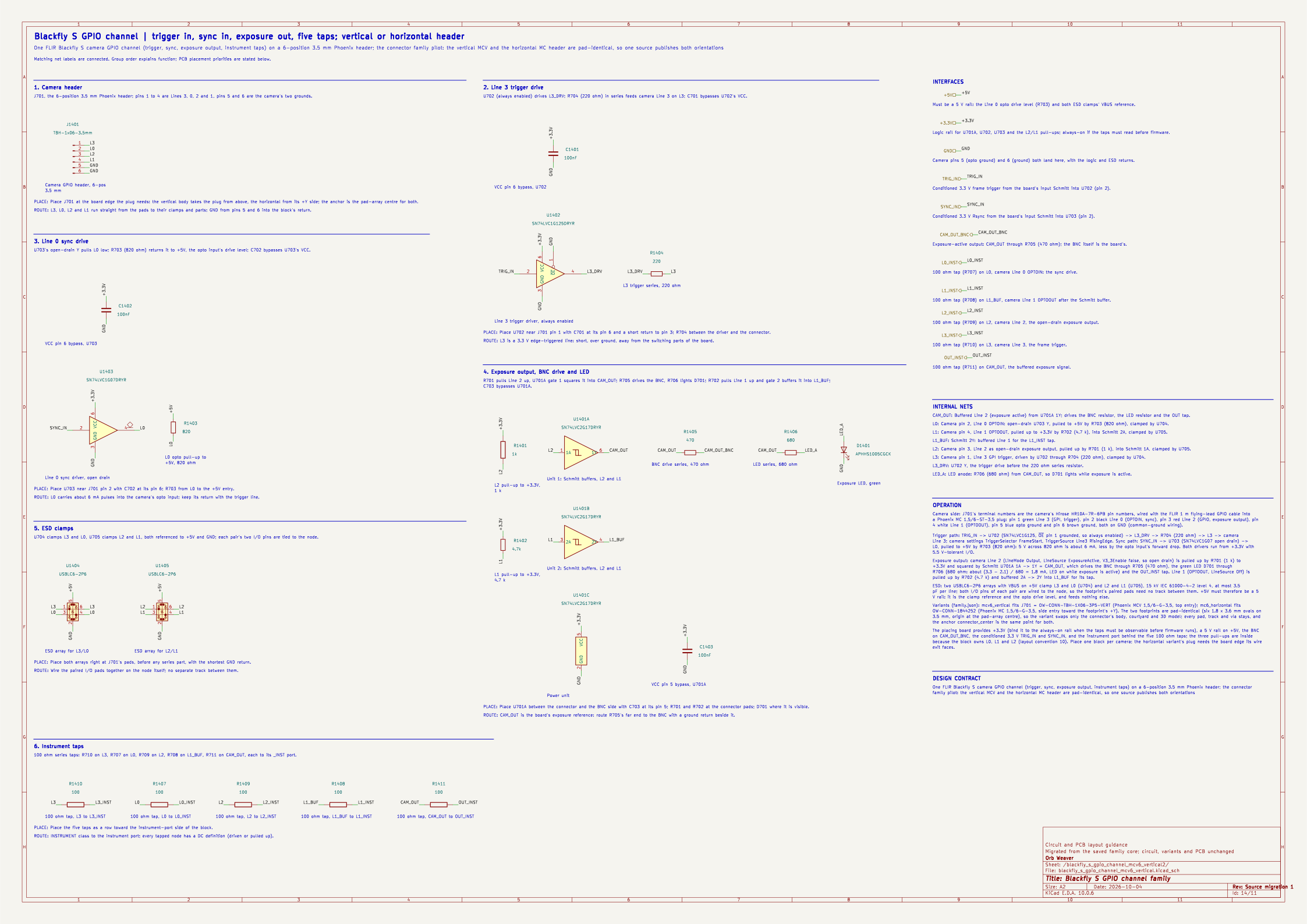
Block orb_weaver_blackfly_s_gpio_channel:blackfly_s_gpio_channel_mcv6_vertical placed in / of camera-gpio-interface-pcb. One FLIR Blackfly S camera GPIO channel (trigger, sync, exposure output, instrument taps) on a 6-position 3.5 mm Phoenix header; the connector family pilot: the vertical MCV and the horizontal MC header are pad-identical, so one source publishes both orientations
| Lifecycle | routed |
| Family | blackfly_s_gpio_channel mcv6_vertical (gpio): VERTICAL, top-entry 6-position 3.5 mm pluggable screw-terminal header, Phoenix MCV 1,5/6-G-3,5 (1843648), LCSC C5443576 |
| Placement | anchor (25, -24) mm, rotation 180°, front side; anchor rule: inferred (block not in the anchor table): the group's one connector, pad-array centre |
| Sheet | blackfly_s_gpio_channel_mcv6_vertical.kicad_sch; sheet pins: the library's arrangement |
| Drawing | camera-gpio-interface-pcb-blackfly_s_gpio_channel_mcv6_vertical2.svg |
On the Board
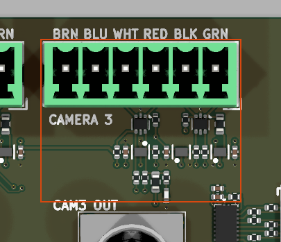
Block 3 of the board view: 23.4 × 19.1 mm on the top side, its centre 25.0 mm right of and 18.0 mm above the board centre (X right, Y up, as the enclosure tables); 21 footprints. The picture is the top render clipped around the block, the rectangle the extent of its footprints' courtyards.
Description
One FLIR Blackfly S camera GPIO channel on a VERTICAL, top-entry 6-position 3.5 mm pluggable screw-terminal header, Phoenix MCV 1,5/6-G-3,5 (1843648), LCSC C5443576: 6-position 3.5mm pluggable terminal block header, vertical top-entry plug-in, rated 8A 160V; OW-CONN-TBH-1X06-3P5-VERT, footprint orb_weaver_tht:PhoenixContact_MCV_1,5_6-G-3.5_1x06_P3.50mm_Vertical. The vertical and horizontal headers share one pad pattern, so both variants carry the same copper and differ in the connector's body, courtyard and wire exit only. Place one per camera. TERMINAL NUMBERS ARE THE CAMERA'S HIROSE HR10A-7R-6PB PIN NUMBERS, wired with the FLIR 1 m flying-lead GPIO cable into a Phoenix MC 1,5/6-ST-3,5 plug (1840405): 1 green Line 3 (GPI, non-isolated input), 2 black Line 0 (OPTOIN, opto-isolated input), 3 red Line 2 (GPIO, non-isolated open-drain output here), 4 white Line 1 (OPTOOUT, opto-isolated output), 5 blue opto ground, 6 brown ground. Both grounds land on the block's GND: this is the COMMON-GROUND variant, matching how the rig already runs; an isolated variant is a different block, not a population option. Common to every cased Blackfly S (BFS-U3 and BFS-PGE) with the 6-pin GPIO; other FLIR families use different connectors and line sets and need their own blocks. LINE ASSIGNMENT IS FIXED IN COPPER AND IS THE POINT OF THE BLOCK. TRIG_IN (frame trigger, 150 Hz on the rig) goes to Line 3, the fast input (high 2.6 to 3.6 V, 1 us propagation): SN74LVC1G125 U23002 (OW-MISC-SN74LVC1G125DRYR, C527546, ~OE grounded) at 3.3 V through R23004 220 ohm 0603 (OW-PASS-0603WAF2200T5E, C22962), a per-camera driver so a shorted cable pulls one channel down, not all three; 220 ohm bounds that fault to 15 mA and 50 mW (hence 1/10 W 0603) and slows the edge to about 25 ns into a 1 m lead, still far faster than the camera's 1 us input. SYNC_IN (Rsync, 25 ms pulses) goes to Line 0, the opto input (18 us L-H, 9 us H-L; identity matters, not microseconds): SN74LVC1G07 open-drain U23003 (OW-MISC-SN74LVC1G07DRYR, C2675513) at 3.3 V with R23003 820 ohm (OW-PASS-FRC0402F8200TS, C2909387) from the Line 0 node to +5V. Signal high, buffer off, the opto LED sees FLIR's documented test condition of 5 V through 1 kohm, about 4 mA against the 3.5 to 7 mA specification; signal low, the buffer sinks the 820 ohm (about 0.15 V, 27 mW continuous in the resistor while Rsync idles low). FLIR publishes no internal circuit for this input, so the block reproduces the specified condition rather than the rig's empirical bare 3.3 V drive. +5V MUST BE A 5 V RAIL: it is the opto drive level and the ESD clamp reference, and it feeds nothing but R23003 and the two VBUS pins. The 1G07 open-drain output is rated to 5.5 V independent of VCC. CAM_OUT comes from Line 2 as an open-drain output (1 us, real FET, about 0.2 V low): R23001 1 kohm (OW-PASS-RC0402FR-071KL, C106235) to +3.3V, 3.1 mA when the camera pulls low, into SN74LVC2G17 U23001 gate 1 (OW-MISC-SN74LVC2G17DRYR, C2675856). THIS COSTS THE CAMERA'S VOUT: SET V3_3Enable FALSE ON LINE 2, LineMode Output, LineSource ExposureActive. If V3_3Enable is left on nothing is damaged, the camera's own 3.3 V simply holds the node high through the 1 kohm and CAM_OUT reads stuck high until it is switched off. Line 1 (OPTOOUT, 36 us L-H, 18 us H-L) is NOT the BNC source: it goes through R23002 4.7 kohm (OW-RES-4K7-0402, C25900) to +3.3V into 2G17 gate 2 as L1_BUF for the InstrumentPort only. The pull-up is weak on purpose: FLIR measures OPTOOUT low at 0.92 V with 5 V/1 kohm and 1.47 V with 3.3 V/200 ohm, roughly 200 ohm of internal drop, so about 0.6 mA keeps the low near 0.4 V, under the Schmitt's worst-case 0.8 V VT-. The three pull-ups live inside the block because the block owns the camera-facing nodes; nothing here pulls TRIG_IN or SYNC_IN, so three instances sharing those inputs do not parallel any resistor. CAM_OUT_BNC is CAM_OUT through R23005 470 ohm 0603 (OW-PASS-0603WAF4700T5E, C23179); the BNC itself stays on the board sheet. 470 ohm, not 220 and not 50: the OneBox shares each ADC pin with a +/-5 V 20 mA DAC through a software switch, and a DAC left enabled holds the far end at the ESD clamp, about -0.8 or +5.5 V, so the resistor sees up to 5.5 V continuously: 12 mA through the driver (24 mA recommended sink) and 64 mW in the resistor (0603 is 100 mW); 220 ohm would be 25 mA and 137 mW, 50 ohm a 66 mA short. OUTPUT IS FIXED AT 3.3 V, no 5 V option, because anything that may one day be fed back into a pyControl BNC has to stay under that board's 3.3 V clamps. Activity LED D23001 APHHS1005CGCK (OW-MISC-APHHS1005CGCK, C2853065) through R23006 680 ohm (OW-PASS-RC0402FR-07680RL, C137948), about 1.8 mA, lit while exposure is active, so it reads steadily half-lit at 150 Hz. ESD IS TWO USBLC6-2P6 ARRAYS, NOT ONE: the part is TWO-LINE, pins 1/6 are one internal node and 3/4 the other. U23004 protects Line 3 (pins 1, 6) and Line 0 (pins 3, 4); U23005 protects Line 2 (pins 1, 6) and Line 1 (pins 3, 4); both VBUS pins on +5V because the Line 0 node swings to about 4.7 V; both pins of each pair are wired to the node. Use only orb_weaver_smd:USBLC6-2P6_SOT-666 (OW-MISC-USBLC6-2P6, C2827693), whose jumper pad groups match the symbol. Putting four lines on one array shorts them in pairs. INSTRUMENT TAPS: five 100 ohm T-taps (OW-PASS-0402WGF1000TCE, C25076) from L3 (R23010), L0 (R23007), L2 (R23009), L1_BUF (R23008) and CAM_OUT (R23011) to ports L3_INST, L0_INST, L2_INST, L1_INST, OUT_INST, following the mouse-joystick tap rules: 100 ohm on timing signals, _INST suffix on block pins and board nets alike, INSTRUMENT netclass from the instrument-taps profile. L0_INST swings 0 to 4.7 V, inside the digital-50 DUT block's 5.5 V tolerant LV541A inputs. Every tap node is driven or pulled up, so no _INST net needs its own pull. PORTS: in TRIG_IN, SYNC_IN, +3.3V, +5V, GND; out CAM_OUT_BNC, L3_INST, L0_INST, L2_INST, L1_INST, OUT_INST. +3.3V is the only logic rail; bind it to the board's always-on rail when the taps must be observable before firmware runs. Not in the block: the BNC, the input Schmitt conditioning and 100 kohm pull-downs (quadrature_encoder_input_5v_sn74lvc2g17), the SYNC OUT driver. DECOUPLING is one 100 nF per package (OW-CAP-100N-0402-X5R-16V, C162178): C23001 at U23002 pin 6, C23002 at U23003 pin 6, C23003 at U23001 pin 5, each hard against its VCC pin with a short return; there is no bulk capacitor, the board's rail supplies it. CAMERA SETTINGS THAT GO WITH THIS BLOCK: TriggerSelector FrameStart, TriggerSource Line3, RisingEdge; Line 0 LineMode Input (Rsync, read as ExposureEndLineStatusAll bit 0); Line 2 LineMode Output, LineSource ExposureActive, V3_3Enable false; Line 1 LineSource Off or a diagnostic source. Apply with TriggerMode Off, re-save UserSet0 as default. DRY6 land pattern (three per channel) is unproven until a board assembles; the MCV 6 vertical rotation row in vendor_specs/jlcpcb/footprint-rotations.csv was promoted 2026-09-28 from the camera board's placement preview. LAYOUT: one copper for both connector variants, 118 track segments and 26 vias all 0.6 mm / 0.3 mm (9 GND, 6 +3.3V, 3 +5V, one escape via on each of the eight signal ports), no zones; the User.1 boundary follows the placed connector's courtyard; judged at publication (release.json). Pairs with instrument_port_digital_50_dut_ffc_boundary_vertical for the taps; the board-level BNC ESD needs two more USBLC6-2P6 for four output BNCs. GPIO profile. +5V MUST BE A 5 V RAIL: it is the opto drive level and the ESD clamp reference. +3.3V is the only logic rail; bind it to the board's always-on rail when the taps must be observable before firmware runs. Camera settings that go with this block: TriggerSelector FrameStart, TriggerSource Line3 RisingEdge; Line 0 LineMode Input; Line 2 LineMode Output, LineSource ExposureActive, V3_3Enable false; Line 1 LineSource Off. The horizontal variant's plug enters from the side (+Y of the footprint, connector-datums.json): give it the board edge the wire exit needs; the vertical's plug enters from above
Ports
The brief's shape, edge, class and meaning for each port, then what the board wires it to.
| Port | Shape | Edge | Class | Wired to | Board net | Board class | GPIO | Meaning | On this board |
|---|---|---|---|---|---|---|---|---|---|
+3.3V |
passive | west | PWR_3V3_LOCAL | +3.3V |
/+3.3V |
PWR_3V3_NARROW | Logic rail for U23001, U23002, U23003 and the L2/L1 pull-ups; always-on if the taps must read before firmware. | The only logic rail, from the TPS73733 on the power sheet; always on while USB is present, as the InstrumentPort block requires | |
+5V |
passive | west | PWR_5V_LOCAL | +5V |
/+5V |
PWR_5V_NARROW | Must be a 5 V rail: the Line 0 opto drive level (R23003) and both ESD clamps' VBUS reference. | VBUS after the USB block's Schottky (+5V_USB in the design record): the Line 0 pull-ups and every ESD array's clamp reference | |
CAM_OUT_BNC |
output | west | Default | CAM3_OUT_BNC |
/CAM3_OUT_BNC |
Default | Exposure-active output: CAM_OUT through R23005 (470 ohm); the BNC itself is the board's. | Camera 3 ExposureActive (Line 2, Schmitt-buffered) behind the block's 470 Ω, to the CAM3 OUT BNC | |
GND |
passive | west | PWR_RETURN_LOCAL | GND |
/GND |
PWR_RETURN_LOCAL | Camera pins 5 (opto ground) and 6 (ground) both land here, with the logic and ESD returns. | Board ground; every BNC shell and camera pins 5 and 6 | |
L0_INST |
output | west | INSTRUMENT | CAM3_L0_INST |
/CAM3_L0_INST |
INSTRUMENT | 100 ohm tap (R23007) on L0, camera Line 0 OPTOIN: the sync drive. | DIG13: camera 3 pin 2 node (Line 0, the Rsync drive), 0 to 4.7 V open-drain | |
L1_INST |
output | west | INSTRUMENT | CAM3_L1_INST |
/CAM3_L1_INST |
INSTRUMENT | 100 ohm tap (R23008) on L1_BUF, camera Line 1 OPTOOUT after the Schmitt buffer. | DIG14: camera 3 OPTOOUT (Line 1), Schmitt-buffered; a second camera output for diagnosing missed triggers | |
L2_INST |
output | west | INSTRUMENT | CAM3_L2_INST |
/CAM3_L2_INST |
INSTRUMENT | 100 ohm tap (R23009) on L2, camera Line 2, the open-drain exposure output. | DIG15: camera 3 Line 2 raw open-drain node (ExposureActive) | |
L3_INST |
output | west | INSTRUMENT | CAM3_L3_INST |
/CAM3_L3_INST |
INSTRUMENT | 100 ohm tap (R23010) on L3, camera Line 3, the frame trigger. | DIG16: camera 3 pin 1 node (Line 3, the trigger) after the 220 Ω | |
OUT_INST |
output | west | INSTRUMENT | CAM3_OUT_INST |
/CAM3_OUT_INST |
INSTRUMENT | 100 ohm tap (R23011) on CAM_OUT, the buffered exposure signal. | DIG17: what the CAM3 OUT BNC carries | |
SYNC_IN |
input | west | Default | SYNC_IN |
/SYNC_IN |
Default | Conditioned 3.3 V Rsync from the board's input Schmitt into U23003 (pin 2). | Conditioned Rsync from the SYNC IN BNC, 3.3 V, to the three Line 0 drivers and the SYNC OUT driver | |
TRIG_IN |
input | west | Default | TRIG_IN |
/TRIG_IN |
Default | Conditioned 3.3 V frame trigger from the board's input Schmitt into U23002 (pin 2). | Conditioned 150 Hz frame trigger from the TRIG IN BNC, 3.3 V, to the three camera channels' Line 3 drivers |
Parts
As placed on the board's sheet; 21 of 21 paired with the brief's references by symbol identity, the rest given the brief's role where the internal part has one, else the catalog's role slug; the placement is the Placement field of the board's symbol, else of the library's (D38); the manufacturer part and the LCSC number are the board's BOM's.
| Reference | Brief | Part | Value | Role | Placement | Manufacturer part | LCSC | DNP |
|---|---|---|---|---|---|---|---|---|
C1201 |
C23001 |
OW-CAP-100N-0402-X5R-16V |
100nF | VCC pin 6 bypass, U23002 | beside U1202.6 (VCC), on +3.3V | GRM155R62A104KE14D | C162178 | |
C1202 |
C23002 |
OW-CAP-100N-0402-X5R-16V |
100nF | VCC pin 6 bypass, U23003 | beside U1203.6 (VCC), on +3.3V | GRM155R62A104KE14D | C162178 | |
C1203 |
C23003 |
OW-CAP-100N-0402-X5R-16V |
100nF | VCC pin 5 bypass, U23001 | beside U1201C.5 (VCC), on +3.3V | GRM155R62A104KE14D | C162178 | |
D1201 |
D23001 |
OW-MISC-APHHS1005CGCK |
APHHS1005CGCK | Exposure LED, green | APHHS1005CGCK | C2853065 | ||
J1201 |
J23001 |
OW-CONN-TBH-1X06-3P5-VERT |
TBH-1x06-3.5mm | Camera GPIO header, 6-pos 3.5 mm | 1843648 | C5443576 | ||
R1201 |
R23001 |
OW-PASS-RC0402FR-071KL |
1k | L2 pull-up to +3.3V, 1 k | beside U1201A.1 (1A), on L2 | RC0402FR-071KL | C106235 | |
R1202 |
R23002 |
OW-RES-4K7-0402 |
4.7k | L1 pull-up to +3.3V, 4.7 k | beside U1201B.3 (2A), on L1 | 0402WGF4701TCE | C25900 | |
R1203 |
R23003 |
OW-PASS-FRC0402F8200TS |
820 | L0 opto pull-up to +5V, 820 ohm | beside U1203.4, on L0 | FRC0402F8200TS | C2909387 | |
R1204 |
R23004 |
OW-PASS-0603WAF2200T5E |
220 | L3 trigger series, 220 ohm | 0603WAF2200T5E | C22962 | ||
R1205 |
R23005 |
OW-PASS-0603WAF4700T5E |
470 | BNC drive series, 470 ohm | 0603WAF4700T5E | C23179 | ||
R1206 |
R23006 |
OW-PASS-RC0402FR-07680RL |
680 | LED series, 680 ohm | RC0402FR-07680RL | C137948 | ||
R1207 |
R23007 |
OW-PASS-0402WGF1000TCE |
100 | 100 ohm tap, L0 to L0_INST | 0402WGF1000TCE | C25076 | ||
R1208 |
R23008 |
OW-PASS-0402WGF1000TCE |
100 | 100 ohm tap, L1_BUF to L1_INST | 0402WGF1000TCE | C25076 | ||
R1209 |
R23009 |
OW-PASS-0402WGF1000TCE |
100 | 100 ohm tap, L2 to L2_INST | 0402WGF1000TCE | C25076 | ||
R1210 |
R23010 |
OW-PASS-0402WGF1000TCE |
100 | 100 ohm tap, L3 to L3_INST | 0402WGF1000TCE | C25076 | ||
R1211 |
R23011 |
OW-PASS-0402WGF1000TCE |
100 | 100 ohm tap, CAM_OUT to OUT_INST | 0402WGF1000TCE | C25076 | ||
U1201 |
U23001 |
OW-MISC-SN74LVC2G17DRYR |
SN74LVC2G17DRYR | Schmitt buffers, L2 and L1 | SN74LVC2G17DRYR | C2675856 | ||
U1202 |
U23002 |
OW-MISC-SN74LVC1G125DRYR |
SN74LVC1G125DRYR | Line 3 trigger driver, always enabled | SN74LVC1G125DRYR | C527546 | ||
U1203 |
U23003 |
OW-MISC-SN74LVC1G07DRYR |
SN74LVC1G07DRYR | Line 0 sync driver, open drain | SN74LVC1G07DRYR | C2675513 | ||
U1204 |
U23004 |
OW-MISC-USBLC6-2P6 |
USBLC6-2P6 | ESD array for L3/L0 | USBLC6-2P6 | C2827693 | ||
U1205 |
U23005 |
OW-MISC-USBLC6-2P6 |
USBLC6-2P6 | ESD array for L2/L1 | USBLC6-2P6 | C2827693 |
Operating Notes
- Camera side: J23001's terminal numbers are the camera's Hirose HR10A-7R-6PB pin numbers, wired with the FLIR 1 m flying-lead GPIO cable into a Phoenix MC 1,5/6-ST-3,5 plug: pin 1 green Line 3 (GPI, trigger), pin 2 black Line 0 (OPTOIN, sync), pin 3 red Line 2 (GPIO, exposure output), pin 4 white Line 1 (OPTOOUT), pin 5 blue opto ground and pin 6 brown ground, both on GND (common-ground wiring).
- Trigger path: TRIG_IN -> U23002 (SN74LVC1G125, ~{OE} pin 1 grounded, so always enabled) -> L3_DRV -> R23004 (220 ohm) -> L3 -> camera Line 3; camera settings TriggerSelector FrameStart, TriggerSource Line3 RisingEdge. Sync path: SYNC_IN -> U23003 (SN74LVC1G07 open drain) -> L0, pulled to +5V by R23003 (820 ohm): 5 V across 820 ohm is about 6 mA, less by the opto input's forward drop. Both drivers run from +3.3V with 5.5 V-tolerant I/O.
- Exposure output: camera Line 2 (LineMode Output, LineSource ExposureActive, V3_3Enable false, so open drain) is pulled up by R23001 (1 k) to +3.3V and squared by Schmitt U23001 1A -> 1Y = CAM_OUT, which drives the BNC through R23005 (470 ohm), the green LED D23001 through R23006 (680 ohm: about (3.3 - 2.1) / 680 = 1.8 mA, LED on while exposure is active) and the OUT_INST tap. Line 1 (OPTOOUT, LineSource Off) is pulled up by R23002 (4.7 k) and buffered 2A -> 2Y into L1_BUF for its tap.
- ESD: two USBLC6-2P6 arrays with VBUS on +5V clamp L3 and L0 (U23004) and L2 and L1 (U23005), 15 kV IEC 61000-4-2 level 4, at most 3.5 pF per line; both I/O pins of each pair are wired to the node, so the footprint's paired pads need no track between them. +5V must therefore be a 5 V rail: it is the clamp reference and the opto drive level, and feeds nothing else.
- Variants (family.json): mcv6_vertical fits J23001 = OW-CONN-TBH-1X06-3P5-VERT (Phoenix MCV 1,5/6-G-3,5, top entry); mc6_horizontal fits OW-CONN-1844252 (Phoenix MC 1,5/6-G-3,5, side entry toward the footprint's +Y). The two footprints are pad-identical (six 1.8 x 3.6 mm ovals on 3.5 mm, origin at the pad-array centre), so the variant swaps only the connector's body, courtyard and 3D model; every pad, track and via stays, and the anchor connector_center is the same point for both.
- The placing board provides +3.3V (bind it to the always-on rail when the taps must be observable before firmware runs), a 5 V rail on +5V, the BNC on CAM_OUT_BNC, the conditioned 3.3 V TRIG_IN and SYNC_IN, and the instrument port behind the five 100 ohm taps; the three pull-ups are inside because the block owns L0, L1 and L2 (layout convention 10). Place one block per camera; the horizontal variant's plug needs the board edge its wire exit faces.
Placement and Routing
Camera header
J23001
J23001, the 6-position 3.5 mm Phoenix header; pins 1 to 4 are Lines 3, 0, 2 and 1, pins 5 and 6 are the camera's two grounds.
- Place: Place J23001 at the board edge the plug needs: the vertical body takes the plug from above, the horizontal from its +Y side; the anchor is the pad-array centre for both.
- Route: L3, L0, L2 and L1 run straight from the pads to their clamps and parts; GND from pins 5 and 6 into the block's return.
Line 3 trigger drive
U23002, R23004, C23001
U23002 (always enabled) drives L3_DRV; R23004 (220 ohm) in series feeds camera Line 3 on L3; C23001 bypasses U23002's VCC.
- Place: Place U23002 near J23001 pin 1 with C23001 at its pin 6 and a short return to pin 3; R23004 between the driver and the connector.
- Route: L3 is a 3.3 V edge-triggered line: short, over ground, away from the switching parts of the board.
Line 0 sync drive
U23003, R23003, C23002
U23003's open-drain Y pulls L0 low; R23003 (820 ohm) returns it to +5V, the opto input's drive level; C23002 bypasses U23003's VCC.
- Place: Place U23003 near J23001 pin 2 with C23002 at its pin 6; R23003 from L0 to the +5V entry.
- Route: L0 carries about 6 mA pulses into the camera's opto input; keep its return with the trigger line.
Exposure output, BNC drive and LED
U23001, R23001, R23002, R23005, R23006, D23001, C23003
R23001 pulls Line 2 up, U23001 gate 1 squares it into CAM_OUT; R23005 drives the BNC, R23006 lights D23001; R23002 pulls Line 1 up and gate 2 buffers it into L1_BUF; C23003 bypasses U23001.
- Place: Place U23001 between the connector and the BNC side with C23003 at its pin 5; R23001 and R23002 at the connector pads; D23001 where it is visible.
- Route: CAM_OUT is the board's exposure reference: route R23005's far end to the BNC with a ground return beside it.
ESD clamps
U23004, U23005
U23004 clamps L3 and L0, U23005 clamps L2 and L1, both referenced to +5V and GND; each pair's two I/O pins are tied to the node.
- Place: Place both arrays right at J23001's pads, before any series part, with the shortest GND return.
- Route: Wire the paired I/O pads together on the node itself; no separate track between them.
Instrument taps
R23010, R23007, R23009, R23008, R23011
100 ohm series taps: R23010 on L3, R23007 on L0, R23009 on L2, R23008 on L1_BUF, R23011 on CAM_OUT, each to its _INST port.
- Place: Place the five taps as a row toward the instrument-port side of the block.
- Route: INSTRUMENT class to the instrument port; every tapped node has a DC definition (driven or pulled up).
Library Identity
| Block | orb_weaver_blackfly_s_gpio_channel:blackfly_s_gpio_channel_mcv6_vertical |
| Resolution | the placed id is in the library |
| Brief | design_block_families/blackfly_s_gpio_channel/source/blackfly_s_gpio_channel.brief.yaml, the family's brief |
| Published sheet | c9f98b3dd751f5b0 |
| Published PCB | bc94c2fa85826a2e |
| Family release | blackfly_s_gpio_channel variant mcv6_vertical, profile gpio; VERTICAL, top-entry 6-position 3.5 mm pluggable screw-terminal header, Phoenix MCV 1,5/6-G-3,5 (1843648), LCSC C5443576; geometry 76343d3e1fe7bf57; copper 5697f9a330d24bc3; hardware unvalidated; qualification matches |
| Placed sheet | c66fa0c5aaaae95b: matches the brief: its 21 parts by internal part, every port by name and shape; the file is the board's copy under its own designators |
| Netlist check | ok on 2026-10-15: every pin on the brief's net; 24 identity records differ, the board's own instances |